Advanced Nintendo Entertainment System (ANES) – NES Modded to Use 2 PPUs
Summary
This repository provides schematics and instructions for modifying the original Nintendo Entertainment System to use two PPU chips, enabling enhanced graphics like more colors, more sprites, and parallax scrolling.
View Cached Full Text
Cached at: 06/25/26, 08:13 PM
decrazyo/anes
Source: https://github.com/decrazyo/anes
Advanced Nintendo Entertainment System (ANES)
This repo outlines the process for modding the NES to use 2 PPUs for advanced graphical features. I don’t expect anyone to actually bother building this so the docs might be kind of half-assed at times. Check out my modified fork of Mesen2 if you’d like to play with this concept without modding your NES. See the related projects section for some demos that take advantage of the dual-PPU setup.
Features
- More colors!
- More sprites!
- Parallax scrolling!
Schematics

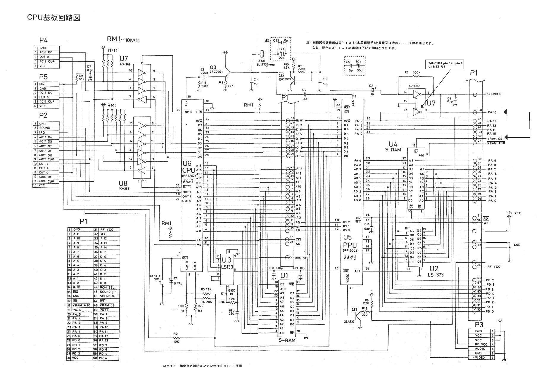
KiCad files can be found in the hardware directory.
Materials
You’ll want to start with two consoles. One to modify and another as a parts donor.
| quantity | location | part number | description |
|---|---|---|---|
| 2 | U1, U2 | RP2C02 | PPUs desoldered from both consoles |
| 1 | U3 | AS6C6264-55PCN | Static RAM for PPU2 |
| 1 | U4 | 74LS373 | Address latch desoldered from donor console |
| 1 | U5 | 74LS139 | Demultiplexer desoldered from donor console |
| 1 | U1 | EMS-26405 | 40 pin wire wrap socket for PPU1 |
| 2 | J1 | 20 pin female pin headers to receive the wire wrap socket | |
| 1 | U5/J3 | 16 pin socket for 74LS139 | |
| 4 | RN1 | 10K 1/4 watt EXT pull down resitors | |
| 1 | 6x8cm prototype board | ||
| 1 | U2 | 40 pin socket for PPU2 (optional) | |
| 1 | U3 | 28 pin socket for AS6C6264-55PCN (optional) | |
| 1 | U4 | 20 pin socket for 74LS373 (optional) |
Build
1. Cut Prototype Board
The 6x8cm prototype boards listed in the materials section is slightly too large and interferes with the expansion port.

2. Desolder the Following
- RP2C02 (U5) from the console you want to modify and your donor console.

- 74LS373 (U2) from your donor console.

- 74LS139 (U3) from your donor console.

3. Move Capacitors
These capacitors may be in the way of the dual-PPU board.

Fold them down flat or relocate them to the other side of the motherboard.

4. Solder Headers
Solder 2 20 pin female headers where the PPU used to be.
5. Build the Dual-PPU Board
Follow the provided schematics and photos to assemble the dual-PPU board. Good luck.


4. Install the Demultiplexer
remove pins 6, 7, 9, 10, 11, 12, 13, 14, and 15 from a 16 pin IC socket.
Bend pins 2, 3, 4, and 5 out horizontally.
Attach the socket on top of the console’s 74LS139, soldering the remaining pins 1, 8, and 16.
Solder a jumper wire from pin 2 of the socket to CPU address line A12

Solder a jumper wire from pin 3 of the socket to the console’s 74LS139 pin 5

Solder a jumper wire from pins 4 and 5 of the socket to the /CE pins of PPU1 and PPU2 respectively.
Install your donor 74LS139 in the socket.

5. Install Dual-PPU board
Plug the dual-PPU board into the female pin headers. You’re done.
Related Projects
- https://github.com/decrazyo/Mesen2
- https://github.com/decrazyo/dual-ppu-demo
- https://github.com/VinglesSmi/DualPPUTest
Similar Articles
How the SNES Graphics System works
A detailed technical explanation of the Super Nintendo's graphics hardware, including the PPU1 and PPU2 chips, VRAM, OAM, and CGRAM, based on schematics by Jonathon Donaldson.
SNES: Sprites and backgrounds rendering
The article explains how the SNES PPUs render sprites and backgrounds under tight VRAM bandwidth constraints, describing the hardware trade-offs in different video modes.
The evolution of the Super Nintendo motherboard
This article details the evolution of Super Nintendo motherboard revisions over its 12-year lifespan, highlighting how Nintendo reduced the number of chips from fifteen to nine through generations like Classic, APU, and 1-CHIP.
Carving the Super Nintendo Video System
A detailed exploration of the Super Nintendo's video system design, explaining CRT technology and engineering choices from a Nintendo engineer's perspective.
Inside the Super Nintendo cartridges
A detailed technical analysis of Super Nintendo cartridges, covering CIC copy protection, ROM size distribution, SRAM with battery backup, and enhancement processors like the Super FX chip.