A detailed reverse-engineering analysis of how the Intel 8087 floating-point coprocessor decodes instructions, explaining the interplay between the main CPU and coprocessor, the use of microcode ROM, and the bus interface unit.
<style>
pre {border:none;}
</style>
In the 1980s, if you wanted your IBM PC to run faster, you could buy
the Intel 8087 floating-point coprocessor chip.
With this chip, CAD software, spreadsheets, flight simulators, and other programs
were much speedier.
The 8087 chip could add, subtract, multiply, and divide, of course, but it could
also compute
transcendental functions such as tangent and logarithms, as well as provide
constants such as π.
In total, the 8087 added 62 new instructions to the computer.</p>
<p>But how does a PC decide if an instruction was
a floating-point instruction for the 8087 or a regular instruction for the 8086 or 8088 CPU?
And how does the 8087 chip interpret instructions to determine what they mean?
It turns out that decoding an instruction inside the 8087 is more complicated than you might expect.
The 8087 uses multiple techniques, with decoding circuitry spread across the chip.
In this blog post, I'll explain how these decoding circuits work.</p>
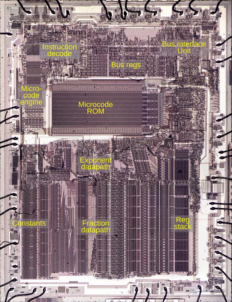
<p>To reverse-engineer the 8087, I chiseled open the ceramic package of an 8087 chip and took numerous photos of the silicon die with a microscope.
The complex patterns on the die are formed by its metal wiring, as well as the polysilicon and silicon underneath.
The bottom half of the chip is the "datapath", the circuitry that performs calculations on 80-bit floating point values.
At the left of the datapath, a <a href="https://www.righto.com/2020/05/extracting-rom-constants-from-8087-math.html">constant ROM</a> holds important constants such as π.
At the right are the eight registers that the
programmer uses to hold floating-point values; in an unusual design decision,
these registers are arranged as a <a href="https://www.righto.com/2025/12/8087-stack-circuitry.html">stack</a>.
Floating-point numbers cover a huge range by representing numbers with a fractional part and an exponent;
the 8087 has separate circuitry to process the fractional part and the exponent.</p>
<p><a href="https://static.righto.com/images/8087-decode/8087-die-labeled.jpg"><img alt="Die of the Intel 8087 floating point unit chip, with main functional blocks labeled. The die is 5 mm×6 mm. Click this image (or any others) for a larger image." class="hilite" height="587" src="https://static.righto.com/images/8087-decode/8087-die-labeled-w450.jpg" title="Die of the Intel 8087 floating point unit chip, with main functional blocks labeled. The die is 5 mm×6 mm. Click this image (or any others) for a larger image." width="450" /></a><div class="cite">Die of the Intel 8087 floating point unit chip, with main functional blocks labeled. The die is 5 mm×6 mm. Click this image (or any others) for a larger image.</div></p>
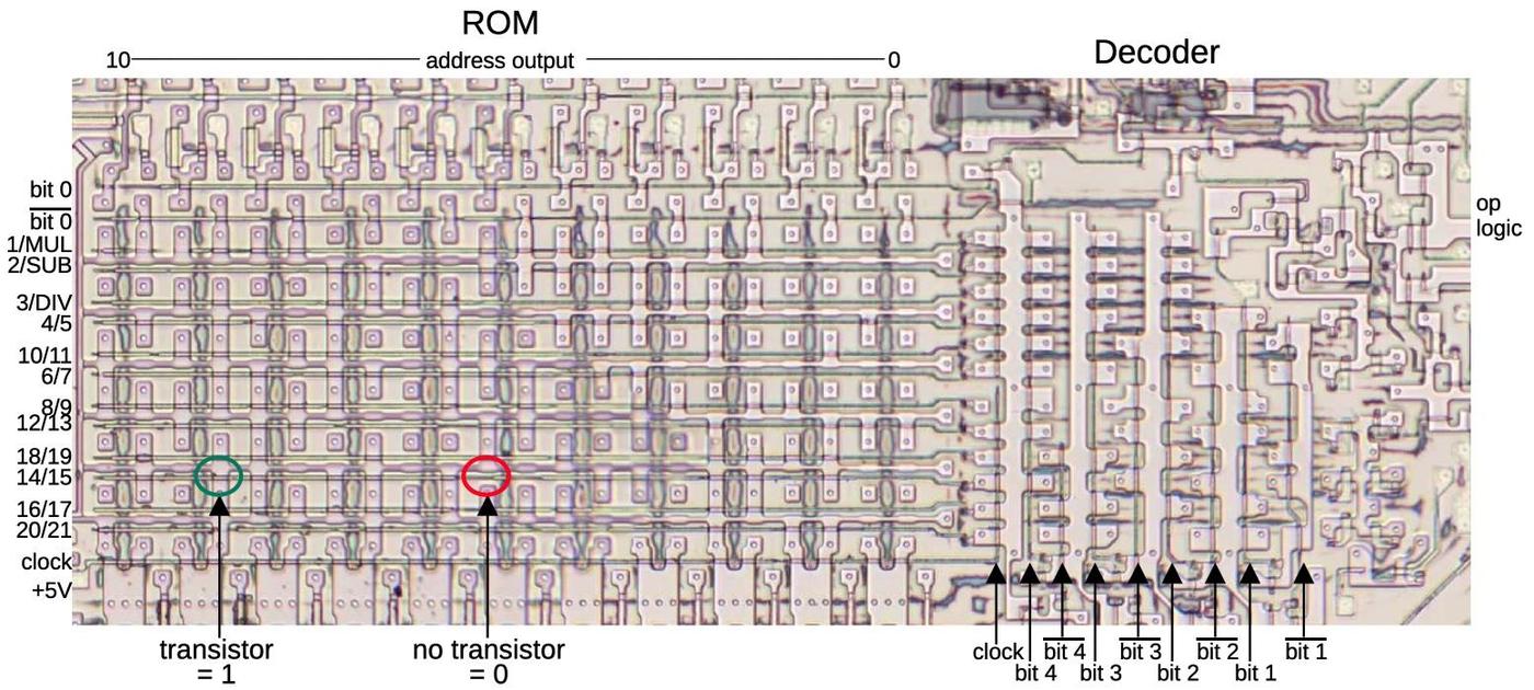
<p>The chip's instructions are defined by the large <a href="https://www.righto.com/2018/09/two-bits-per-transistor-high-density.html">microcode ROM</a> in the middle.<span id="fnref:microcode"><a class="ref" href="#fn:microcode">1</a></span>
To execute an instruction, the 8087 decodes the instruction and the microcode engine starts executing
the appropriate micro-instructions from the microcode ROM.
In the upper right part of the chip, the Bus Interface Unit (BIU) communicates with the
main processor and memory over the computer's bus.
For the most part, the BIU and the rest of the chip operate independently,
but as we will see, the BIU plays important roles in instruction decoding and execution.</p>
<h2>Cooperation with the main 8086/8088 processor</h2>
<p>The 8087 chip acted as a coprocessor with the main 8086 (or 8088) processor. When a floating-point instruction was encountered,
the 8086 would let the 8087 floating-point chip carry out the floating-point instruction.
But how do the 8086 and the 8087 determine which chip executes a particular instruction?
You might expect the 8086 to tell the 8087 when it should execute an instruction, but
this cooperation turns out to be more
complicated.</p>
<p>The 8086 has eight opcodes that are assigned to the coprocessor, called <code>ESCAPE</code> opcodes.
The 8087 determines what instruction the 8086 is executing by watching the bus,
a task performed by the BIU (Bus Interface Unit).<span id="fnref:queue"><a class="ref" href="#fn:queue">2</a></span>
If the instruction is an <code>ESCAPE</code>, the instruction is intended for the 8087.
However, there's a problem. The 8087 doesn't have any access to the 8086's registers (and vice versa), so the only way
that they can exchange data is through memory.
But the 8086 addresses memory through a complicated scheme involving offsest registers and segment registers.
How can the 8087 determine what memory address to use when it doesn't have access to the registers?</p>
<p>The trick is that when an <code>ESCAPE</code> instruction is encountered,
the 8086 processor starts executing the instruction, even though it is intended for the 8087.
The 8086 computes the memory address that the instruction references and
reads that memory address, but ignores the result.
Meanwhile, the 8087 watches the memory bus to see what address is accessed and stores this address internally in a BIU register.
When the 8087 starts executing the instruction, it uses the address from the 8086 to read and write
memory.
In effect, the 8087 offloads address computation to the 8086 processor.</p>
<h2>The structure of 8087 instructions</h2>
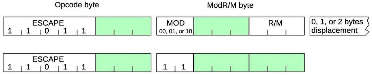
<p>To understand the 8087's instructions, we need to take a closer look at the structure of 8086
instructions. In particular, something called the ModR/M byte is important since all 8087 instructions
use it.</p>
<p>The 8086 uses a complex system of opcodes with a mixture of single-byte opcodes, prefix bytes, and longer instructions.
About a quarter of the opcodes use a second byte, called ModR/M,
that specifies the registers and/or memory address
to use through a complicated encoding.
For instance, the memory address can be computed by adding the BX and SI registers, or from the BP register plus a two-byte offset.
The first two bits of the ModR/M byte are the "MOD" bits. For a memory access, the MOD bits indicate
how many address displacement bytes follow the ModR/M byte (0, 1, or 2), while
the "R/M" bits specify how the address is computed.
A MOD value of 3, however, indicates that the instruction operates on registers and does
not access memory.</p>
<p><a href="https://static.righto.com/images/8087-decode/modrm.jpg"><img alt="Structure of an 8087 instruction" class="hilite" height="122" src="https://static.righto.com/images/8087-decode/modrm-w600.jpg" title="Structure of an 8087 instruction" width="600" /></a><div class="cite">Structure of an 8087 instruction</div></p>
<p>The diagram above shows how an 8087 instruction consists of an <code>ESCAPE</code> opcode, followed by
a ModR/M byte.
An <code>ESCAPE</code> opcode is indicated by the special bit pattern <code>11011</code>, leaving three bits (green) available
in the first byte to specify the type of 8087 instruction.
As mentioned above, the ModR/M byte has two forms.
The first form performs a memory access; it has MOD bits of <code>00</code>,<code>01</code>, or <code>10</code> and the R/M bits
specify how the memory address is computed. This leaves three bits (green) to specify the address.
The second form operates internally, without a memory access; it has MOD bits of <code>11</code>.
Since the R/M bits aren't used in the second form, six bits (green) are available in the R/M byte
to specify the instruction.</p>
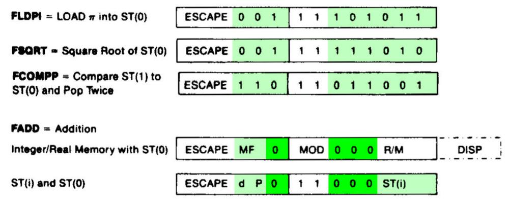
<p>The challenge for the designers of the 8087 was to fit all the instructions into the available bits
in such a way that decoding is straightforward.
The diagram below shows a few 8087 instructions, illustrating how they achieve this.
The first three instructions operate internally, so they have MOD bits of 11; the green
bits specify the particular instruction.
Addition is more complicated because it can act on memory (first format) or registers (second format), depending on the <code>MOD</code> bits.
The four bits highlighted in bright green (<code>0000</code>) are the same for all <code>ADD</code> instructions;
the subtract, multiplication, and division instructions use the same structure but have
different values for
the dark green bits. For instance, <code>0001</code> indicates multiplication and <code>0100</code> indicates subtraction.
The other green bits (<code>MF</code>, <code>d</code>, and <code>P</code>) select variants of the addition instruction,
changing the data format, direction, and popping the stack at the end.
The last three bits select the R/M addressing mode for a memory operation, or the stack register
<code>ST(i)</code> for a register operation.</p>
<p><a href="https://static.righto.com/images/8087-decode/opcodes.jpg"><img alt="The bit patterns for some 8087 instructions. Based on the datasheet." class="hilite" height="200" src="https://static.righto.com/images/8087-decode/opcodes-w500.jpg" title="The bit patterns for some 8087 instructions. Based on the datasheet." width="500" /></a><div class="cite">The bit patterns for some 8087 instructions. Based on the <a href="https://datasheets.chipdb.org/Intel/x86/808x/datashts/8087/205835-007.pdf#page=20">datasheet</a>.</div></p>
<h2>Selecting a microcode routine</h2>
<p>Most of the 8087's instructions are implemented in microcode, implementing each step of
an instruction in low-level "micro-instructions".
The 8087 chip contains a microcode engine; you can think of it as the mini-CPU
that controls the 8087 by executing a microcode routine, one micro-instruction at a time.
The microcode engine provides an 11-bit micro-address to the ROM, specifying the micro-instruction
to execute.
Normally, the microcode engine steps through the microcode sequentially, but it also supports conditional
jumps and subroutine calls.</p>
<p>But how does the microcode engine know where to start executing the microcode for a particular machine instruction?
Conceptually, you could feed the instruction opcode into a ROM that would provide the starting micro-address.
However, this would be impractical since you'd need a 2048-word ROM to decode an 11-bit opcode.<span id="fnref:opcode"><a class="ref" href="#fn:opcode">3</a></span>
(While a 2K ROM is small nowadays, it was large at the time; the 8087's microcode ROM
was a tight fit at just 1648 words.)
Instead, the 8087 uses a more efficient (but complicated) instruction decode system constructed from a combination of logic gates and
PLAs (Programmable Logic Arrays).
This system holds 22 microcode entry points, much more practical than 2048.</p>
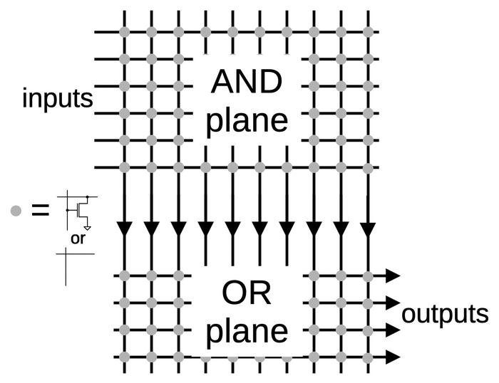
<p>Processors often use a circuit called a PLA (Programmable Logic Array) as part of instruction decoding.
The idea of a PLA is to provide a dense and flexible way of implementing arbitrary logic functions.
Any Boolean logic function can be expressed as a "sum-of-products", a collection of AND terms (products) that are OR'd together (summed).
A PLA has a block of circuitry called the AND plane that generates the desired sum terms.
The outputs of the AND plane are fed into a second block, the OR plane, which ORs the terms together.
Physically, a PLA is implemented as a grid, where each spot in the grid can either have a
transistor or not.
By changing the transistor pattern, the PLA implements the desired function.</p>
<p><a href="https://static.righto.com/images/8087-decode/pla-structure.jpg"><img alt="A simplified diagram of a PLA." class="hilite" height="269" src="https://static.righto.com/images/8087-decode/pla-structure-w350.jpg" title="A simplified diagram of a PLA." width="350" /></a><div class="cite">A simplified diagram of a PLA.</div></p>
<p>A PLA can implement arbitrary logic, but in the 8087, PLAs often act as optimized
ROMs.<span id="fnref:rom"><a class="ref" href="#fn:rom">4</a></span> The AND plane matches bit patterns,<span id="fnref:matching"><a class="ref" href="#fn:matching">5</a></span> selecting an entry from the OR plane, which
holds the output values, the micro-address for each routine.
The advantage of the PLA over a standard ROM is that one output column can be used for many different inputs, reducing the size.</p>
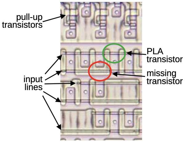
<p>The image below shows part of the instruction decoding PLA.<span id="fnref:pla-layout"><a class="ref" href="#fn:pla-layout">6</a></span>
The horizontal input lines are polysilicon wires on top of the silicon.
The pinkish regions are doped silicon.
When polysilicon crosses doped silicon, it creates a transistor (green).
Where there is a gap in the doped silicon, there is no transistor (red).
(The output wires run vertically, but are not visible here;
I dissolved the metal layer to show the silicon underneath.)
If a polysilicon line is energized, it turns on all the transistors in its row, pulling
the associated output columns to ground. (If no transistors are turned on, the pull-up transistor
pulls the output high.)
Thus, the pattern of doped silicon regions creates a grid of transistors in the PLA that
implements the desired logic function.<span id="fnref:nor"><a class="ref" href="#fn:nor">7</a></span></p>
<p><a href="https://static.righto.com/images/8087-decode/pla-diagram.jpg"><img alt="Part of the PLA for instruction decoding." class="hilite" height="231" src="https://static.righto.com/images/8087-decode/pla-diagram-w300.jpg" title="Part of the PLA for instruction decoding." width="300" /></a><div class="cite">Part of the PLA for instruction decoding.</div></p>
<p>The standard way to decode instructions with a PLA is to take the instruction bits (and their complements) as inputs.
The PLA can then pattern-match against bit patterns in the instruction.
However, the 8087 also uses some pre-processing to reduce the size of the PLA.
For instance, the <code>MOD</code> bits are processed to generate a signal if the bits are 0, 1, or 2 (i.e.
a memory operation) and a second signal if the bits are 3 (i.e. a register operation).
This allows the 0, 1, and 2 cases to be handled by a single PLA pattern.
Another signal indicates that the top bits are <code>001 111xxxxx</code>; this indicates that the R/M field
takes part in instruction selection.<span id="fnref:table"><a class="ref" href="#fn:table">8</a></span>
Sometimes a PLA output is fed back in as an input, so a decoded group of instructions can be
excluded from another group.
These techniques all reduce the size of the PLA at the cost of some additional logic gates.</p>
<p>The result of the instruction decoding PLA's AND plane is 22 signals, where each signal
corresponds to an
instruction or group of instructions with a shared microcode entry point.
The lower part of the instruction decoding PLA acts as a ROM that holds the 22 microcode entry points
and provides the selected one.<span id="fnref:entry-points"><a class="ref" href="#fn:entry-points">9</a></span></p>
<h2>Instruction decoding inside the microcode</h2>
<p>Many 8087 instructions share the same microcode routines. For instance,
the addition, subtraction, multiplication, division, reverse subtraction, and reverse division instructions all go to the same microcode routine.
This reduces the size of the microcode since these instructions share the microcode that sets up the instruction and handles the
result.
However, the microcode obviously needs to diverge at some point to perform the specific operation.
Moreover, some arithmetic opcodes access the top of the stack, some access an arbitrary location in the stack, some access memory, and some reverse the operands, requiring
different microcode actions.
How does the microcode do different things for different opcodes while sharing code?</p>
<p>The trick is that the 8087's microcode engine supports conditional subroutine calls, returns, and jumps, based on 49 different
conditions (<a href="https://www.righto.com/2025/12/8087-microcode-conditions.html">details</a>).
In particular, fifteen conditions examine the instruction.
Some conditions test specific bit patterns, such as branching if the lowest bit is set, or more complex patterns such as
an opcode matching <code>0xx 11xxxxxx</code>. Other conditions detect specific instructions such as <code>FMUL</code>.
The result is that the microcode can take different paths for different instructions. For instance, a reverse subtraction or
reverse division is implemented in the microcode by testing the instruction and reversing the arguments if necessary, while sharing the rest of the code.</p>
<p>The microcode also has a special jump target that performs a three-way jump depending on the
current machine instruction that is being executed.
The microcode engine has a jump ROM that holds 22 entry points for jumps or subroutine calls.<span id="fnref:jump"><a class="ref" href="#fn:jump">10</a></span>
However, a jump to target 0 uses special circuitry so it will instead jump to
target 1
for a multiplication instruction,
target 2 for an addition/subtraction, or
target 3 for division.
This special jump is implemented by gates in the upper right corner of the jump decoder.</p>
<p><a href="https://static.righto.com/images/8087-decode/jump-rom.jpg"><img alt="The jump decoder and ROM. Note that the rows are not in numerical order; presumably, this made the layout slightly more compact. Click this image (or any other) for a larger version." class="hilite" height="315" src="https://static.righto.com/images/8087-decode/jump-rom-w700.jpg" title="The jump decoder and ROM. Note that the rows are not in numerical order; presumably, this made the layout slightly more compact. Click this image (or any other) for a larger version." width="700" /></a><div class="cite">The jump decoder and ROM. Note that the rows are not in numerical order; presumably, this made the layout slightly more compact. Click this image (or any other) for a larger version.</div></p>
<h2>Hardwired instruction handling</h2>
<p>Some of the 8087's instructions are implemented directly by hardware in the Bus Interface Unit (BIU), rather than using microcode.
For example, instructions to enable or disable interrupts, or to save or restore state are implemented in hardware.
The decoding for these instructions is performed by separate circuitry from the instruction decoder described above.</p>
<p>In the first step, a small PLA decodes the top 5 bits of the instruction.
Most importantly, if these bits are <code>11011</code>, it indicates an ESCAPE instruction, the start of
an 8087 operation. This causes the 8087 to start interpreting the instruction and stores
the opcode in a BIU register for use
by the instruction decoder.
A second small PLA takes the outputs from the top-5 PLA and combines them with the lower three bits.
It decodes specific instruction values:
<code>D9</code>, <code>DB</code>, <code>DD</code>, <code>E0</code>, <code>E1</code>, <code>E2</code>, or <code>E3</code>.
The first three values correspond to specific ESCAPE instructions,
and are recorded in latches.</p>
<p>The two PLAs decode the second byte in the same way.
Logic gates combine the PLA outputs from the second byte with the latched values from the first byte,
detecting eleven hardwired instructions.<span id="fnref:control"><a class="ref" href="#fn:control">11</a></span>
Some of these instructions operate directly on registers, such as clearing exceptions;
the decoded instruction signal
goes to the relevant register and modifies it in an ad hoc way. <span id="fnref:fclex"><a class="ref" href="#fn:fclex">12</a></span>.
Other hardwired instructions are more complicated, writing chip state to memory or reading chip state from memory.
These instructions require multiple memory operations, controlled by the Bus Interface Unit's state machine.
Each of these instructions has a flip-flop that is triggered by the decoded instruction to keep track of which instruction is active.</p>
<p>For the instructions that save and restore the 8087's state (<code>FSAVE</code> and <code>FRSTOR</code>), there's one more complication.
These instructions are partially implemented in the BIU, which moves the relevant BIU registers to or from memory.
But then, instruction processing switches to microcode, where a microcode routine saves
or loads the floating-point registers.
Jumping to the microcode routine is not implemented through the regular microcode jump circuitry.
Instead, two hardcoded values force the microcode address to the save or restore routine.<span id="fnref:save"><a class="ref" href="#fn:save">13</a></span></p>
<h2>Constants</h2>
<p>The 8087 has seven instructions to load floating-point constants such as π, 1, or log<sub>10</sub>(2).
The 8087 has a constant ROM that holds these constants, as well as constants for transcendental
operations.
You might expect that the 8087 simply loads the specified constant from the constant ROM, using
the instruction to select the desired constant.
However, the process is much more complicated.<span id="fnref:constants"><a class="ref" href="#fn:constants">14</a></span></p>
<p>Looking at the instruction decode ROM shows that different constants are implemented with different
microcode routines: the constant-loading instructions <code>FLDLG2</code> and <code>FLDLN2</code> have one entry
point; <code>FLD1</code>, <code>FLD2E</code>, <code>FLDL2T</code>, and <code>FLDPI</code> have a second entry point, and <code>FLDZ</code> (zero) has a third entry point.
It's understandable that zero is a special case, but why are there two routines for the other constants?</p>
<p>The explanation is that the fraction part of each constant is stored in the constant ROM, but the
exponent is stored in a separate, smaller ROM.
To reduce the size of the exponent ROM, only some of the necessary exponents are stored.
If a constant needs an exponent one larger than a value in the ROM, the microcode adds one to the
exponent ROM value, computing the exponent on the fly.</p>
<p>Thus, the load-constant instructions use three separate instruction decoding mechanisms.
First, the instruction decode ROM determines the appropriate microcode routine for the constant
instruction, as before.
Then, the constant PLA decodes the instruction to select the appropriate constant.
Finally, the microcode routine tests the bottom bit of the instruction and increments the
exponent if necessary.</p>
<h2>Conclusions</h2>
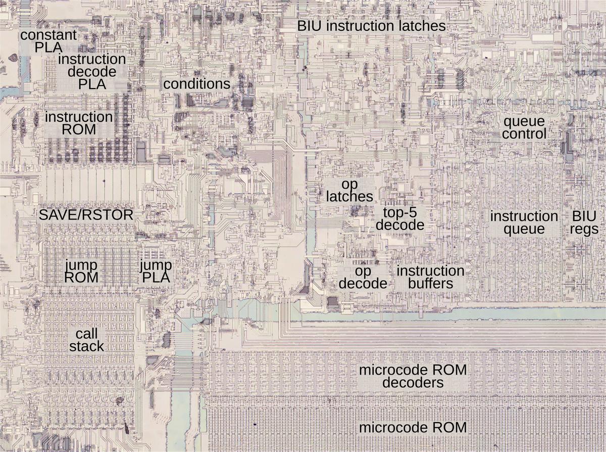
<p>To wrap up the discussion of the decoding circuitry, the diagram below shows how the
different circuits are arranged on the die. This image shows the upper-right part of the die;
the microcode engine is at the left and part of the ROM is at the bottom.</p>
<p><a href="https://static.righto.com/images/8087-decode/decoding-labeled.jpg"><img alt="The upper-left portion of the 8087 die, with functional blocks labeled." class="hilite" height="447" src="https://static.righto.com/images/8087-decode/decoding-labeled-w600.jpg" title="The upper-left portion of the 8087 die, with functional blocks labeled." width="600" /></a><div class="cite">The upper-left portion of the 8087 die, with functional blocks labeled.</div></p>
<p>The 8087 doesn't have a clean architecture, but instead is full of ad hoc circuits and corner
cases.
The 8087's instruction decoding is an example of this.
Decoding is complicated to start with due to the 8086's convoluted instruction
formats and the ModR/M byte.
On top of that, the 8087's instruction decoding has multiple layers: the instruction decode PLA,
microcode conditional jumps that depend on the instruction, a special jump target that
depends on the instruction,
constants selected based on the instruction, and instructions decoded by the BIU.</p>
<p>The 8087 has a reason for this complicated architecture: at the time, the chip was on the
edge of what was possible, so the designers needed to use whatever techniques they could to
reduce the size of the chip. If implementing a corner case could shave a few transistors off the
chip or make the microcode ROM slightly smaller, the corner case was worthwhile.
Even so, the 8087 was barely manufacturable at first; early yield was just two working chips
per silicon wafer.
Despite this difficult start, a floating-point standard based on the 8087 is now part of almost every processor.</p>
<p>Thanks to the members of the "Opcode Collective" for their contributions, especially Smartest Blob and Gloriouscow.</p>
<p>For updates, follow me on
Bluesky (<a href="https://bsky.app/profile/righto.com">@righto.com</a>),
Mastodon (<a href="https://oldbytes.space/@kenshirriff">@[email protected]</a>),
or <a href="http://www.righto.com/feeds/posts/default">RSS</a>.</p>
<h2>Notes and references</h2>
<div class="footnote">
<ol>
<li id="fn:microcode">
<p>The contents of the microcode ROM are available <a href="https://github.com/a-mcego/granite/blob/main/tools/8087mc/bin/8087mc_out.txt">here</a>, partially decoded thanks to Smartest Blob. <a class="footnote-backref" href="#fnref:microcode" title="Jump back to footnote 1 in the text">↩</a></p>
</li>
<li id="fn:queue">
<p>It is difficult for the 8087 to determine what the 8086 is doing because the 8086 prefetches
instructions. Thus, when an instruction is seen on the bus, the 8086 may execute it at some
point in the future, or it may end up discarded.</p>
<p>In order to tell what instruction is being executed, the 8087 floating-point chip internally duplicates the 8086 processor's queue.
The 8087 watches the memory bus and copies any instructions that are prefetched.
Since the 8087 can't tell from the bus when the 8086 starts a new instruction or when the 8086 empties the queue when jumping to a new address,
the 8086 processor provides two queue status signals to the 8087.
With the help of these signals, the 8087 knows exactly what the 8086 is executing.</p>
<p>The 8087's instruction queue has six 8-bit registers, the same as the 8086.
Surprisingly, the last two queue registers in the 8087 are tied together, so there are
only five usable queue registers.
My hypothesis is that since the 8087 copies the active instruction into separate registers
(unlike the 8086), only five queue registers are needed. This raises the question of
why the excess register wasn't removed from the die, rather than wasting valuable space.</p>
<p>The 8088 processor, used in the IBM PC, has a four-byte queue instead of a six-byte queue. The 8088 is almost identical to the 8086
except it has an 8-bit memory bus instead of a 16-bit memory bus. With the narrower memory bus, prefetching is more likely to get in
the way of other memory accesses, so a smaller prefetch queue was implemented.</p>
<p>Knowing the queue size is essential to the 8087 floating-point chip.
To indicate this, when the processor boots, a signal lets the 8087 determine if the attached processor is
an 8086 or an 8088. <a class="footnote-backref" href="#fnref:queue" title="Jump back to footnote 2 in the text">↩</a></p>
</li>
<li id="fn:opcode">
<p>The relevant part of the opcode is 11 bits:
the top 5 bits are always
<code>11011</code> for an <code>ESCAPE</code> opcode, so they can be ignored during decoding.
The Bus Interface Unit has a 3-bit register to hold the
first byte of the instruction and an 8-bit register to hold the second byte.
The BIU registers have an irregular appearance because there are 3-bit registers, 8-bit
registers, and 10-bit registers (holding half of a 20-bit address). <a class="footnote-backref" href="#fnref:opcode" title="Jump back to footnote 3 in the text">↩</a></p>
</li>
<li id="fn:rom">
<p>What's the difference between a PLA and a ROM?
There is a lot of overlap: a ROM can replace a PLA, while a PLA can implement a ROM.
A ROM is essentially a PLA where the first stage is a binary decoder, so the ROM
has a separate row for each input value.
However, the first stage of a ROM can be optimized so multiple inputs share the same output value;
is this a ROM or a PLA?</p>
<p>The "official" difference is that in a ROM, one row is activated at a time, while in a PLA,
multiple rows can be activated at once, so the output values are combined.
(Thus, it is straightforward to read the values out of a ROM, but more difficult to read
the values out of a PLA.)</p>
<p>I consider the instruction decoding PLA to be best described as a PLA first stage with the
second stage acting as a ROM.
You could also call it a partially-decoded ROM, or just a PLA.
Hopefully my terminology isn't too confusing. <a class="footnote-backref" href="#fnref:rom" title="Jump back to footnote 4 in the text">↩</a></p>
</li>
<li id="fn:matching">
<p>To match a bit pattern in an instruction,
the bits of the instruction are fed into the PLA, along with the complements of these bits; this allows the PLA to match against a 0
bit or a 1 bit.
Each row of a PLA will match a particular bit pattern in the instruction: bits that must be 1, bits that must be 0, and bits that don't matter.
If the instruction opcodes are assigned rationally, a small number of bit patterns will match all the opcodes, reducing the size of the
decoder.</p>
<p>I may be going too far with this analogy, but a PLA is a lot like a neural net. Each column in the AND plane is like a
neuron that fires when it recognizes a particular input pattern.
The OR plane is like a second layer in a neural net, combining signals from the first layer.
The PLA's "weights", however, are fixed at 0 or 1, so it's not as flexible as a "real" neural net. <a class="footnote-backref" href="#fnref:matching" title="Jump back to footnote 5 in the text">↩</a></p>
</li>
<li id="fn:pla-layout">
<p>The instruction decoding PLA has an unusual layout, where the second plane is rotated 90°.
In a regular PLA (left), the inputs (red) go into the first plane, the perpendicular outputs from the first plane (purple) go into the second plane,
and the PLA outputs (blue) exit parallel to the inputs.
In the address PLA, however, the second plane is rotated 90°, so the outputs are perpendicular to the inputs.
This approach requires additional wiring (horizontal purple lines), but presumably, this layout worked better in the 8087 since the outputs are lined up with the rest of the microcode engine.</p>
<p><a href="https://static.righto.com/images/8087-decode/folded.jpg"><img alt="Conceptual diagram of a regular PLA on the left and a rotated PLA on the right." class="hilite" height="265" src="https://static.righto.com/images/8087-decode/folded-w350.jpg" title="Conceptual diagram of a regular PLA on the left and a rotated PLA on the right." width="350" /></a><div class="cite">Conceptual diagram of a regular PLA on the left and a rotated PLA on the right.</div></p>
<p><!-- --> <a class="footnote-backref" href="#fnref:pla-layout" title="Jump back to footnote 6 in the text">↩</a></p>
</li>
<li id="fn:nor">
<p>To describe the implementation of a PLA in more detail, the transistors in each row of the AND plane form a NOR gate, since if any transistor is turned on, it pulls the output low.
Likewise, the transistors in each column of the OR plane form a NOR gate.
So why is the PLA described as having an AND plane and an OR plane, rather than two NOR planes?
By using <a href="https://en.wikipedia.org/wiki/De_Morgan%27s_laws">De Morgan's law</a>, you can treat the NOR-NOR Boolean equations as
equivalent to AND-OR Boolean equations (with the inputs and outputs inverted).
It's usually much easier to understand the logic as AND terms OR'd together.</p>
<p>The converse question is why don't they build the PLA from AND and OR gates instead of NOR gates? The reason is that AND and OR
gates are harder to build with NMOS transistors, since you need to add explicit inverter circuits.
Moreover, NMOS NOR gates are typically faster than NAND gates because the transistors are in parallel. (CMOS is the opposite;
NAND gates are faster because the weaker PMOS transistors are in parallel.) <a class="footnote-backref" href="#fnref:nor" title="Jump back to footnote 7 in the text">↩</a></p>
</li>
<li id="fn:table">
<p><style type="text/css">
table#op8087 {border-collapse: collapse; font-family: sans-serif;}
table#op8087 td {border: 1px solid white;}
</style></p>
<p>The 8087's opcodes can be organized into tables, showing the underlying structure.
(In each table, the row (Y) coordinate is the bottom 3 bits of the first byte and the column (X) coordinate
is the 3 bits after the MOD bits in the second byte.)</p>
<p>Memory operations use the following encoding with MOD = 0, 1, or 2.
Each box represents 8 different addressing modes.</p>
<p><table id="op8087">
<tr><th> </th>
<th>0</th>
<th>1</th>
<th>2</th>
<th>3</th>
<th>4</th>
<th>5</th>
<th>6</th>
<th>7</th>
</tr>
<tr><th>0</th>
<td style="background-color:#FFD6A5">FADD</td>
<td style="background-color:#FDFFB6">FMUL</td>
<td style="background-color:#CAFFBF">FCOM</td>
<td style="background-color:#CAFFBF">FCOMP</td>
<td style="background-color:#9BF6FF">FSUB</td>
<td style="background-color:#9BF6FF">FSUBR</td>
<td style="background-color:#A0C4FF">FDIV</td>
<td style="background-color:#A0C4FF">FDIVR</td>
<tr><th>1</th>
<td style="background-color:#BDB2FF">FLD</td>
<td> </td>
<td style="background-color:#FFC6FF">FST</td>
<td style="background-color:#FFC6FF">FSTP</td>
<td style="background-color:yellow">FLDENV</td>
<td style="background-color:yellow">FLDCW</td>
<td style="background-color:yellow">FSTENV</td>
<td style="background-color:yellow">FSTCW</td>
<tr><th>2</th>
<td style="background-color:#FFD6A5">FIADD</td>
<td style="background-color:#FDFFB6">FIMUL</td>
<td style="background-color:#CAFFBF">FICOM</td>
<td style="background-color:#CAFFBF">FICOMP</td>
<td style="background-color:#9BF6FF">FISUB</td>
<td style="background-color:#9BF6FF">FISUBR</td>
<td style="background-color:#A0C4FF">FIDIV</td>
<td style="background-color:#A0C4FF">FIDIVR</td>
<tr><th>3</th>
<td style="background-color:#BDB2FF">FILD</td>
<td> </td>
<td style="background-color:#FFC6FF">FIST</td>
<td style="background-color:#FFC6FF">FISTP</td>
<td> </td>
<td style="background-color:#BDB2FF">FLD</td>
<td> </td>
<td style="background-color:#FFC6FF">FSTP</td>
<tr><th>4</th>
<td style="background-color:#FFD6A5">FADD</td>
<td style="background-color:#FDFFB6">FMUL</td>
<td style="background-color:#CAFFBF">FCOM</td>
<td style="background-color:#CAFFBF">FCOMP</td>
<td style="background-color:#9BF6FF">FSUB</td>
<td style="background-color:#9BF6FF">FSUBR</td>
<td style="background-color:#A0C4FF">FDIV</td>
<td style="background-color:#A0C4FF">FDIVR</td>
<tr><th>5</th>
<td style="background-color:#BDB2FF">FLD</td>
<td> </td>
<td style="background-color:#FFC6FF">FST</td>
<td style="background-color:#FFC6FF">FSTP</td>
<td style="background-color:yellow">FRSTOR</td>
<td> </td>
<td style="background-color:yellow">FSAVE</td>
<td style="background-color:yellow">FSTSW</td>
<tr><th>6</th>
<td style="background-color:#FFD6A5">FIADD</td>
<td style="background-color:#FDFFB6">FIMUL</td>
<td style="background-color:#CAFFBF">FICOM</td>
<td style="background-color:#CAFFBF">FICOMP</td>
<td style="background-color:#9BF6FF">FISUB</td>
<td style="background-color:#9BF6FF">FISUBR</td>
<td style="background-color:#A0C4FF">FIDIV</td>
<td style="background-color:#A0C4FF">FIDIVR</td>
<tr><th>7</th>
<td style="background-color:#BDB2FF">FILD</td>
<td> </td>
<td style="background-color:#FFC6FF">FIST</td>
<td style="background-color:#FFC6FF">FISTP</td>
<td style="background-color:#BDB2FF">FBLD</td>
<td style="background-color:#BDB2FF">FILD</td>
<td style="background-color:#FFC6FF">FBSTP</td>
<td style="background-color:#FFC6FF">FISTP</td>
</tr>
</table></p>
<p>The important point is that the instruction encoding has a lot of regularity, making the decoding
process easier. For instance, the basic arithmetic operations (<code>FADD</code> through <code>FDIVR</code>) are
repeated on alternating rows.
However, the table also has significant irregularities, which complicate the decoding process.</p>
<p>The register operations (MOD = 3) have a related layout, but there are even more
irregularities.</p>
<p><style type="text/css">
table#op8087 {border-collapse: collapse; font-family: sans-serif;}
table#op8087 td {border: 1px solid white;}
</style></p>
<p><table id="op8087">
<tr><th> </th>
<th>0</th>
<th>1</th>
<th>2</th>
<th>3</th>
<th>4</th>
<th>5</th>
<th>6</th>
<th>7</th>
</tr>
<tr><th>0</th>
<td style="background-color:#FFD6A5">FADD</td>
<td style="background-color:#FDFFB6">FMUL</td>
<td style="background-color:#CAFFBF">FCOM</td>
<td style="background-color:#CAFFBF">FCOMP</td>
<td style="background-color:#9BF6FF">FSUB</td>
<td style="background-color:#9BF6FF">FSUBR</td>
<td style="background-color:#A0C4FF">FDIV</td>
<td style="background-color:#A0C4FF">FDIVR</td>
<tr><th>1</th>
<td style="background-color:#BDB2FF">FLD</td>
<td style="background-color:#ECDCB0">FXCH</td>
<td style="background-color:#ccc">FNOP</td>
<td> </td>
<td style="background-color:#FFADAD">misc1</td>
<td style="background-color:#FFADAD">misc2</td>
<td style="background-color:#FFADAD">misc3</td>
<td style="background-color:#FFADAD">misc4</td>
<tr><th>2</th>
<td> </td>
<td> </td>
<td> </td>
<td> </td>
<td> </td>
<td> </td>
<td> </td>
<td> </td>
<tr><th>3</th>
<td> </td>
<td> </td>
<td> </td>
<td> </td>
<td style="background-color:yellow">misc5</td>
<td> </td>
<td> </td>
<td> </td>
<tr><th>4</th>
<td style="background-color:#FFD6A5">FADD</td>
<td style="background-color:#FDFFB6">FMUL</td>
<td> </td>
<td> </td>
<td style="background-color:#9BF6FF">FSUB</td>
<td style="background-color:#9BF6FF">FSUBR</td>
<td style="background-color:#A0C4FF">FDIV</td>
<td style="background-color:#A0C4FF">FDIVR</td>
<tr><th>5</th>
<td style="background-color:#EDDCB0">FFREE</td>
<td> </td>
<td style="background-color:#FFC6FF">FST</td>
<td style="background-color:#FFC6FF">FSTP</td>
<td> </td>
<td> </td>
<td> </td>
<td> </td>
<tr><th>6</th>
<td style="background-color:#FFD6A5">FADDP</td>
<td style="background-color:#FDFFB6">FMULP</td>
<td> </td>
<td style="background-color:#CAFFBF">FCOMPP</td>
<td style="background-color:#9BF6FF">FSUBP</td>
<td style="background-color:#9BF6FF">FSUBRP</td>
<td style="background-color:#A0C4FF">FDIVP</td>
<td style="background-color:#A0C4FF">FDIVRP</td>
<tr><th>7</th>
<td> </td>
<td> </td>
<td> </td>
<td> </td>
<td> </td>
<td> </td>
<td> </td>
<td> </td>
</tr>
</table></p>
<p>In most cases, each box indicates 8 different values for the stack register, but there
are exceptions.
The <code>NOP</code> and <code>FCOMPP</code> instructions each have a single opcode, "wasting" the rest of
the box.</p>
<p>Five of the boxes in the table encode multiple instructions instead of the register number.
The first four (red) are miscellaneous instructions handled by the decoding PLA:
<br>
misc1 = <code>FCHS</code>, <code>FABS</code>, <code>FTST</code>, <code>FXAM</code>
<br>
misc2 = <code>FLD1</code>, <code>FLDL2T</code>, <code>FLDL2E</code>, <code>FLDPI</code>, <code>FLDLG2</code>, <code>FLDLN2</code>, <code>FLDZ</code> (the constant-loading instructions)
<br>
misc3 = <code>F2XM1</code>, <code>FYL2X</code>, <code>FPTAN</code>, <code>FPATAN</code>, <code>FXTRACT</code>, <code>FDECSTP</code>, <code>FINCSTP</code>
<br>
misc4 =
<code>FPREM</code>, <code>FYL2XP1</code>, <code>FSQRT</code>, <code>FRNDINT</code>, <code>FSCALE</code></p>
<p>The last miscellaneous box (yellow) holds instructions that are handled by the BIU.
<br>
<code>misc5 = FENI</code>, <code>FDISI</code>, <code>FCLEX</code>, <code>FINIT</code></p>
<p>Curiously, the 8087's opcodes (like the <a href="https://web.archive.org/web/20050329195235/http://www.dabo.de/ccc99/www.camp.ccc.de/radio/help.txt">8086's</a>) make much more sense in octal than in
hexadecimal.
In octal, an 8087 opcode is simply <code>33Y MXR</code>, where X and Y are the table coordinates above,
M is the MOD value (0, 1, 2, or 3), and R is the R/M field or the stack register number. <a class="footnote-backref" href="#fnref:table" title="Jump back to footnote 8 in the text">↩</a></p>
</li>
<li id="fn:entry-points">
<p>The 22 outputs from the instruction decoder PLA correspond to the following groups
of instructions, activating one row of ROM and producing the corresponding microcode address.
From this table, you can see which instructions are grouped together in the microcode.</p>
<p><pre>
0 <a href="https://github.com/a-mcego/granite/blob/main/tools/8087mc/bin/8087mc_out.txt#L201">#0200</a> FXCH
1 <a href="https://github.com/a-mcego/granite/blob/main/tools/8087mc/bin/8087mc_out.txt#L598">#0597</a> FSTP (BCD)
2 <a href="https://github.com/a-mcego/granite/blob/main/tools/8087mc/bin/8087mc_out.txt#L809">#0808</a> FCOM FCOMP FCOMPP
3 <a href="https://github.com/a-mcego/granite/blob/main/tools/8087mc/bin/8087mc_out.txt#L1009">#1008</a> FLDLG2 FLDLN2
4 <a href="https://github.com/a-mcego/granite/blob/main/tools/8087mc/bin/8087mc_out.txt#L1528">#1527</a> FSQRT
5 <a href="https://github.com/a-mcego/granite/blob/main/tools/8087mc/bin/8087mc_out.txt#L1587">#1586</a> FPREM
6 <a href="https://github.com/a-mcego/granite/blob/main/tools/8087mc/bin/8087mc_out.txt#L1139">#1138</a> FPATAN
7 <a href="https://github.com/a-mcego/granite/blob/main/tools/8087mc/bin/8087mc_out.txt#L1040">#1039</a> FPTAN
8 <a href="https://github.com/a-mcego/granite/blob/main/tools/8087mc/bin/8087mc_out.txt#L901">#0900</a> F2XM1
9 <a href="https://github.com/a-mcego/granite/blob/main/tools/8087mc/bin/8087mc_out.txt#L1021">#1020</a> FLDZ
10 <a href="https://github.com/a-mcego/granite/blob/main/tools/8087mc/bin/8087mc_out.txt#L711">#0710</a> FRNDINT
11 <a href="https://github.com/a-mcego/granite/blob/main/tools/8087mc/bin/8087mc_out.txt#L1464">#1463</a> FDECSTP FINCSTP
12 <a href="https://github.com/a-mcego/granite/blob/main/tools/8087mc/bin/8087mc_out.txt#L813">#0812</a> FTST
13 <a href="https://github.com/a-mcego/granite/blob/main/tools/8087mc/bin/8087mc_out.txt#L893">#0892</a> FABS FCHS
14 <a href="https://github.com/a-mcego/granite/blob/main/tools/8087mc/bin/8087mc_out.txt#L66">#0065</a> FFREE FLD
15 <a href="https://github.com/a-mcego/granite/blob/main/tools/8087mc/bin/8087mc_out.txt#L218">#0217</a> FNOP FST FSTP (not BCD)
16 <a href="https://github.com/a-mcego/granite/blob/main/tools/8087mc/bin/8087mc_out.txt#L2">#0001</a> FADD FDIV FDIVR FMUL FSUB FSUBR
17 <a href="https://github.com/a-mcego/granite/blob/main/tools/8087mc/bin/8087mc_out.txt#L749">#0748</a> FSCALE
18 <a href="https://github.com/a-mcego/granite/blob/main/tools/8087mc/bin/8087mc_out.txt#L1029">#1028</a> FXTRACT
19 <a href="https://github.com/a-mcego/granite/blob/main/tools/8087mc/bin/8087mc_out.txt#L1258">#1257</a> FYL2X FYL2XP1
20 <a href="https://github.com/a-mcego/granite/blob/main/tools/8087mc/bin/8087mc_out.txt#L1004">#1003</a> FLD1 FLDL2E FLDL2T FLDPI
21 <a href="https://github.com/a-mcego/granite/blob/main/tools/8087mc/bin/8087mc_out.txt#L1469">#1468</a> FXAM
</pre> <a class="footnote-backref" href="#fnref:entry-points" title="Jump back to footnote 9 in the text">↩</a></p>
</li>
<li id="fn:jump">
<p>The instruction decoding PLA has 22 entries, and the jump table also has 22 entries.
It's a coincidence that these values are the same.</p>
<p>An entry in the jump table ROM is selected by five bits of the micro-instruction.
The ROM is structured with two 11-bit words per row, interleaved. (It's also a coincidence that there
are 22 bits.)
The upper four bits of the jump number select a row in the ROM, while the bottom bit selects
one of the two rows.</p>
<p>This implementation is modified for target 0, the three-way jump. The first ROM row is selected
for target 0 if the current instruction is multiplication, or for target 1.
The second row is selected for target 0 if the current instruction is addition or subtraction,
or for target 2.
The third row is selected for target 0 if the current instruction is division,
or for target 3.
Thus, target 0 ends up selecting rows 1, 2, or 3.
However, remember that there are two words per row, selected by the low bit of the target number.
The problem is that target 0 with multiplication will access the left word of row 1, while
target 1 will access the right word of row 1, but both should provide the same address.
The solution is that rows 1, 2, and 3 have the same address stored twice in the row,
so these rows each "waste" a value.</p>
<p>For reference, the contents of the jump table are:
<pre>
0: Jumps to target 1 for <code>FMUL</code>, 2 for <code>FADD/FSUB/FSUBR</code>, 3 for <code>FDIV/FDIVR</code>
1: <a href="https://github.com/a-mcego/granite/blob/main/tools/8087mc/bin/8087mc_out.txt#L360">#0359</a>
2: <a href="https://github.com/a-mcego/granite/blob/main/tools/8087mc/bin/8087mc_out.txt#L233">#0232</a>
3: <a href="https://github.com/a-mcego/granite/blob/main/tools/8087mc/bin/8087mc_out.txt#L411">#0410</a>
4: <a href="https://github.com/a-mcego/granite/blob/main/tools/8087mc/bin/8087mc_out.txt#L84">#0083</a>
5: <a href="https://github.com/a-mcego/granite/blob/main/tools/8087mc/bin/8087mc_out.txt#L1485">#1484</a>
6: <a href="https://github.com/a-mcego/granite/blob/main/tools/8087mc/bin/8087mc_out.txt#L123">#0122</a>
7: <a href="https://github.com/a-mcego/granite/blob/main/tools/8087mc/bin/8087mc_out.txt#L174">#0173</a>
8: <a href="https://github.com/a-mcego/granite/blob/main/tools/8087mc/bin/8087mc_out.txt#L440">#0439</a>
9: <a href="https://github.com/a-mcego/granite/blob/main/tools/8087mc/bin/8087mc_out.txt#L656">#0655</a>
10: <a href="https://github.com/a-mcego/granite/blob/main/tools/8087mc/bin/8087mc_out.txt#L535">#0534</a>
11: <a href="https://github.com/a-mcego/granite/blob/main/tools/8087mc/bin/8087mc_out.txt#L300">#0299</a>
12: <a href="https://github.com/a-mcego/granite/blob/main/tools/8087mc/bin/8087mc_out.txt#L1573">#1572</a>
13: <a href="https://github.com/a-mcego/granite/blob/main/tools/8087mc/bin/8087mc_out.txt#L1447">#1446</a>
14: <a href="https://github.com/a-mcego/granite/blob/main/tools/8087mc/bin/8087mc_out.txt#L860">#0859</a>
15: <a href="https://github.com/a-mcego/granite/blob/main/tools/8087mc/bin/8087mc_out.txt#L397">#0396</a>
16: <a href="https://github.com/a-mcego/granite/blob/main/tools/8087mc/bin/8087mc_out.txt#L319">#0318</a>
17: <a href="https://github.com/a-mcego/granite/blob/main/tools/8087mc/bin/8087mc_out.txt#L381">#0380</a>
18: <a href="https://github.com/a-mcego/granite/blob/main/tools/8087mc/bin/8087mc_out.txt#L780">#0779</a>
19: <a href="https://github.com/a-mcego/granite/blob/main/tools/8087mc/bin/8087mc_out.txt#L869">#0868</a>
20: <a href="https://github.com/a-mcego/granite/blob/main/tools/8087mc/bin/8087mc_out.txt#L523">#0522</a>
21: <a href="https://github.com/a-mcego/granite/blob/main/tools/8087mc/bin/8087mc_out.txt#L802">#0801</a>
</pre> <a class="footnote-backref" href="#fnref:jump" title="Jump back to footnote 10 in the text">↩</a></p>
</li>
<li id="fn:control">
<p>Eleven instructions are implemented in the BIU hardware.
Four of these are relatively simple, setting or clearing bits:
<code>FINIT</code> (initialize), <code>FENI</code> (enable interrupts), <code>FDISI</code> (disable interrupts),
and <code>FCLEX</code> (clear exceptions).
Six of these are more complicated, storing state to memory or loading state from memory:
<code>FLDCW</code> (load control word), <code>FSTCW</code> (store control word), <code>FSTSW</code> (store status word),
<code>FSTENV</code> (store environment),
<code>FLDENV</code> (load environment), <code>FSAVE</code> (save state), and <code>FRSTOR</code> (restore state).
As explained elsewhere, the last two instructions are partially implemented in microcode. <a class="footnote-backref" href="#fnref:control" title="Jump back to footnote 11 in the text">↩</a></p>
</li>
<li id="fn:fclex">
<p>Even a seemingly trivial instruction uses more circuitry than you might expect.
For instance, after the <code>FCLEX</code> (clear exception) instruction is decoded, the signal goes through nine gates before it clears the exception
bits in the status register. Along the way, it goes through a flip-flop to synchronize the timing,
a gate to combine it with the reset signal, and various inverters and drivers.
Even though these instructions seem like they should complete immediately, they typically take 5 clock cycles due to overhead in the 8087. <a class="footnote-backref" href="#fnref:fclex" title="Jump back to footnote 12 in the text">↩</a></p>
</li>
<li id="fn:save">
<p>I'll give more details here on the circuit that jumps to the save or restore microcode.
The BIU sends two signals to the microcode engine, one to jump to the save code and one to
jump to the restore code.
These signals are buffered and delayed by a capacitor, probably to adjust the timing of the
signal.</p>
<p>In the microcode engine, there are two hardcoded constants for the routines, just above
the jump table; the
BIU signal causes the appropriate constant to go onto the micro-address lines.
Each bit in the address has a pull-up transistor to +5V or a pull-down transistor to ground.
This approach is somewhat inefficient since it requires two transistor sites per bit. In
comparison, the jump address ROM and the instruction address ROM use one transistor site
per bit.
(As in a PLA, each transistor is present or absent as needed, so the number of physical
transistors is less than the number of transistor sites.)</p>
<p><a href="https://static.righto.com/images/8087-decode/capacitors.jpg"><img alt="Two capacitors in the 8087. This photo shows the metal layer with the silicon and polysilicon underneath." class="hilite" height="250" src="https://static.righto.com/images/8087-decode/capacitors-w500.jpg" title="Two capacitors in the 8087. This photo shows the metal layer with the silicon and polysilicon underneath." width="500" /></a><div class="cite">Two capacitors in the 8087. This photo shows the metal layer with the silicon and polysilicon underneath.</div></p>
<p>Since capacitors are somewhat unusual in NMOS circuits, I'll show them in the photo above.
If a polysilicon line crosses over doped silicon, it creates a transistor.
However, if a polysilicon region sits on top of the doped silicon without crossing it, it forms a capacitor instead.
(The capacitance exists for a transistor, too, but the gate capacitance is generally unwanted.) <a class="footnote-backref" href="#fnref:save" title="Jump back to footnote 13 in the text">↩</a></p>
</li>
<li id="fn:constants">
<p>The documentation provides a hint that the microcode to load constants is complicated.
Specifically, the documentation shows that different constants take different amounts of
time to load.
For instance, log<sub>2</sub>(e) takes 18 cycles while log<sub>2</sub>(10) takes 19 cycles and log<sub>10</sub>(2) takes 21 cycles.
You'd expect that pre-computed constants would all take the same time, so the varying times
show that more is happening behind the scenes. <a class="footnote-backref" href="#fnref:constants" title="Jump back to footnote 14 in the text">↩</a></p>
</li>
</ol>
</div>
# Instruction decoding in the Intel 8087 floating-point chip
Source: [http://www.righto.com/2026/02/8087-instruction-decoding.html](http://www.righto.com/2026/02/8087-instruction-decoding.html)
In the 1980s, if you wanted your IBM PC to run faster, you could buy the Intel 8087 floating\-point coprocessor chip\. With this chip, CAD software, spreadsheets, flight simulators, and other programs were much speedier\. The 8087 chip could add, subtract, multiply, and divide, of course, but it could also compute transcendental functions such as tangent and logarithms, as well as provide constants such as π\. In total, the 8087 added 62 new instructions to the computer\.
But how does a PC decide if an instruction was a floating\-point instruction for the 8087 or a regular instruction for the 8086 or 8088 CPU? And how does the 8087 chip interpret instructions to determine what they mean? It turns out that decoding an instruction inside the 8087 is more complicated than you might expect\. The 8087 uses multiple techniques, with decoding circuitry spread across the chip\. In this blog post, I'll explain how these decoding circuits work\.
To reverse\-engineer the 8087, I chiseled open the ceramic package of an 8087 chip and took numerous photos of the silicon die with a microscope\. The complex patterns on the die are formed by its metal wiring, as well as the polysilicon and silicon underneath\. The bottom half of the chip is the "datapath", the circuitry that performs calculations on 80\-bit floating point values\. At the left of the datapath, a[constant ROM](https://www.righto.com/2020/05/extracting-rom-constants-from-8087-math.html)holds important constants such as π\. At the right are the eight registers that the programmer uses to hold floating\-point values; in an unusual design decision, these registers are arranged as a[stack](https://www.righto.com/2025/12/8087-stack-circuitry.html)\. Floating\-point numbers cover a huge range by representing numbers with a fractional part and an exponent; the 8087 has separate circuitry to process the fractional part and the exponent\.
[](https://static.righto.com/images/8087-decode/8087-die-labeled.jpg)
Die of the Intel 8087 floating point unit chip, with main functional blocks labeled\. The die is 5 mm×6 mm\. Click this image \(or any others\) for a larger image\.
The chip's instructions are defined by the large[microcode ROM](https://www.righto.com/2018/09/two-bits-per-transistor-high-density.html)in the middle\.[1](http://www.righto.com/2026/02/8087-instruction-decoding.html#fn:microcode)To execute an instruction, the 8087 decodes the instruction and the microcode engine starts executing the appropriate micro\-instructions from the microcode ROM\. In the upper right part of the chip, the Bus Interface Unit \(BIU\) communicates with the main processor and memory over the computer's bus\. For the most part, the BIU and the rest of the chip operate independently, but as we will see, the BIU plays important roles in instruction decoding and execution\.
## Cooperation with the main 8086/8088 processor
The 8087 chip acted as a coprocessor with the main 8086 \(or 8088\) processor\. When a floating\-point instruction was encountered, the 8086 would let the 8087 floating\-point chip carry out the floating\-point instruction\. But how do the 8086 and the 8087 determine which chip executes a particular instruction? You might expect the 8086 to tell the 8087 when it should execute an instruction, but this cooperation turns out to be more complicated\.
The 8086 has eight opcodes that are assigned to the coprocessor, called`ESCAPE`opcodes\. The 8087 determines what instruction the 8086 is executing by watching the bus, a task performed by the BIU \(Bus Interface Unit\)\.[2](http://www.righto.com/2026/02/8087-instruction-decoding.html#fn:queue)If the instruction is an`ESCAPE`, the instruction is intended for the 8087\. However, there's a problem\. The 8087 doesn't have any access to the 8086's registers \(and vice versa\), so the only way that they can exchange data is through memory\. But the 8086 addresses memory through a complicated scheme involving offsest registers and segment registers\. How can the 8087 determine what memory address to use when it doesn't have access to the registers?
The trick is that when an`ESCAPE`instruction is encountered, the 8086 processor starts executing the instruction, even though it is intended for the 8087\. The 8086 computes the memory address that the instruction references and reads that memory address, but ignores the result\. Meanwhile, the 8087 watches the memory bus to see what address is accessed and stores this address internally in a BIU register\. When the 8087 starts executing the instruction, it uses the address from the 8086 to read and write memory\. In effect, the 8087 offloads address computation to the 8086 processor\.
## The structure of 8087 instructions
To understand the 8087's instructions, we need to take a closer look at the structure of 8086 instructions\. In particular, something called the ModR/M byte is important since all 8087 instructions use it\.
The 8086 uses a complex system of opcodes with a mixture of single\-byte opcodes, prefix bytes, and longer instructions\. About a quarter of the opcodes use a second byte, called ModR/M, that specifies the registers and/or memory address to use through a complicated encoding\. For instance, the memory address can be computed by adding the BX and SI registers, or from the BP register plus a two\-byte offset\. The first two bits of the ModR/M byte are the "MOD" bits\. For a memory access, the MOD bits indicate how many address displacement bytes follow the ModR/M byte \(0, 1, or 2\), while the "R/M" bits specify how the address is computed\. A MOD value of 3, however, indicates that the instruction operates on registers and does not access memory\.
[](https://static.righto.com/images/8087-decode/modrm.jpg)
Structure of an 8087 instruction
The diagram above shows how an 8087 instruction consists of an`ESCAPE`opcode, followed by a ModR/M byte\. An`ESCAPE`opcode is indicated by the special bit pattern`11011`, leaving three bits \(green\) available in the first byte to specify the type of 8087 instruction\. As mentioned above, the ModR/M byte has two forms\. The first form performs a memory access; it has MOD bits of`00`,`01`, or`10`and the R/M bits specify how the memory address is computed\. This leaves three bits \(green\) to specify the address\. The second form operates internally, without a memory access; it has MOD bits of`11`\. Since the R/M bits aren't used in the second form, six bits \(green\) are available in the R/M byte to specify the instruction\.
The challenge for the designers of the 8087 was to fit all the instructions into the available bits in such a way that decoding is straightforward\. The diagram below shows a few 8087 instructions, illustrating how they achieve this\. The first three instructions operate internally, so they have MOD bits of 11; the green bits specify the particular instruction\. Addition is more complicated because it can act on memory \(first format\) or registers \(second format\), depending on the`MOD`bits\. The four bits highlighted in bright green \(`0000`\) are the same for all`ADD`instructions; the subtract, multiplication, and division instructions use the same structure but have different values for the dark green bits\. For instance,`0001`indicates multiplication and`0100`indicates subtraction\. The other green bits \(`MF`,`d`, and`P`\) select variants of the addition instruction, changing the data format, direction, and popping the stack at the end\. The last three bits select the R/M addressing mode for a memory operation, or the stack register`ST\(i\)`for a register operation\.
[](https://static.righto.com/images/8087-decode/opcodes.jpg)
The bit patterns for some 8087 instructions\. Based on the[datasheet](https://datasheets.chipdb.org/Intel/x86/808x/datashts/8087/205835-007.pdf#page=20)\.
## Selecting a microcode routine
Most of the 8087's instructions are implemented in microcode, implementing each step of an instruction in low\-level "micro\-instructions"\. The 8087 chip contains a microcode engine; you can think of it as the mini\-CPU that controls the 8087 by executing a microcode routine, one micro\-instruction at a time\. The microcode engine provides an 11\-bit micro\-address to the ROM, specifying the micro\-instruction to execute\. Normally, the microcode engine steps through the microcode sequentially, but it also supports conditional jumps and subroutine calls\.
But how does the microcode engine know where to start executing the microcode for a particular machine instruction? Conceptually, you could feed the instruction opcode into a ROM that would provide the starting micro\-address\. However, this would be impractical since you'd need a 2048\-word ROM to decode an 11\-bit opcode\.[3](http://www.righto.com/2026/02/8087-instruction-decoding.html#fn:opcode)\(While a 2K ROM is small nowadays, it was large at the time; the 8087's microcode ROM was a tight fit at just 1648 words\.\) Instead, the 8087 uses a more efficient \(but complicated\) instruction decode system constructed from a combination of logic gates and PLAs \(Programmable Logic Arrays\)\. This system holds 22 microcode entry points, much more practical than 2048\.
Processors often use a circuit called a PLA \(Programmable Logic Array\) as part of instruction decoding\. The idea of a PLA is to provide a dense and flexible way of implementing arbitrary logic functions\. Any Boolean logic function can be expressed as a "sum\-of\-products", a collection of AND terms \(products\) that are OR'd together \(summed\)\. A PLA has a block of circuitry called the AND plane that generates the desired sum terms\. The outputs of the AND plane are fed into a second block, the OR plane, which ORs the terms together\. Physically, a PLA is implemented as a grid, where each spot in the grid can either have a transistor or not\. By changing the transistor pattern, the PLA implements the desired function\.
[](https://static.righto.com/images/8087-decode/pla-structure.jpg)
A simplified diagram of a PLA\.
A PLA can implement arbitrary logic, but in the 8087, PLAs often act as optimized ROMs\.[4](http://www.righto.com/2026/02/8087-instruction-decoding.html#fn:rom)The AND plane matches bit patterns,[5](http://www.righto.com/2026/02/8087-instruction-decoding.html#fn:matching)selecting an entry from the OR plane, which holds the output values, the micro\-address for each routine\. The advantage of the PLA over a standard ROM is that one output column can be used for many different inputs, reducing the size\.
The image below shows part of the instruction decoding PLA\.[6](http://www.righto.com/2026/02/8087-instruction-decoding.html#fn:pla-layout)The horizontal input lines are polysilicon wires on top of the silicon\. The pinkish regions are doped silicon\. When polysilicon crosses doped silicon, it creates a transistor \(green\)\. Where there is a gap in the doped silicon, there is no transistor \(red\)\. \(The output wires run vertically, but are not visible here; I dissolved the metal layer to show the silicon underneath\.\) If a polysilicon line is energized, it turns on all the transistors in its row, pulling the associated output columns to ground\. \(If no transistors are turned on, the pull\-up transistor pulls the output high\.\) Thus, the pattern of doped silicon regions creates a grid of transistors in the PLA that implements the desired logic function\.[7](http://www.righto.com/2026/02/8087-instruction-decoding.html#fn:nor)
[](https://static.righto.com/images/8087-decode/pla-diagram.jpg)
Part of the PLA for instruction decoding\.
The standard way to decode instructions with a PLA is to take the instruction bits \(and their complements\) as inputs\. The PLA can then pattern\-match against bit patterns in the instruction\. However, the 8087 also uses some pre\-processing to reduce the size of the PLA\. For instance, the`MOD`bits are processed to generate a signal if the bits are 0, 1, or 2 \(i\.e\. a memory operation\) and a second signal if the bits are 3 \(i\.e\. a register operation\)\. This allows the 0, 1, and 2 cases to be handled by a single PLA pattern\. Another signal indicates that the top bits are`001 111xxxxx`; this indicates that the R/M field takes part in instruction selection\.[8](http://www.righto.com/2026/02/8087-instruction-decoding.html#fn:table)Sometimes a PLA output is fed back in as an input, so a decoded group of instructions can be excluded from another group\. These techniques all reduce the size of the PLA at the cost of some additional logic gates\.
The result of the instruction decoding PLA's AND plane is 22 signals, where each signal corresponds to an instruction or group of instructions with a shared microcode entry point\. The lower part of the instruction decoding PLA acts as a ROM that holds the 22 microcode entry points and provides the selected one\.[9](http://www.righto.com/2026/02/8087-instruction-decoding.html#fn:entry-points)
## Instruction decoding inside the microcode
Many 8087 instructions share the same microcode routines\. For instance, the addition, subtraction, multiplication, division, reverse subtraction, and reverse division instructions all go to the same microcode routine\. This reduces the size of the microcode since these instructions share the microcode that sets up the instruction and handles the result\. However, the microcode obviously needs to diverge at some point to perform the specific operation\. Moreover, some arithmetic opcodes access the top of the stack, some access an arbitrary location in the stack, some access memory, and some reverse the operands, requiring different microcode actions\. How does the microcode do different things for different opcodes while sharing code?
The trick is that the 8087's microcode engine supports conditional subroutine calls, returns, and jumps, based on 49 different conditions \([details](https://www.righto.com/2025/12/8087-microcode-conditions.html)\)\. In particular, fifteen conditions examine the instruction\. Some conditions test specific bit patterns, such as branching if the lowest bit is set, or more complex patterns such as an opcode matching`0xx 11xxxxxx`\. Other conditions detect specific instructions such as`FMUL`\. The result is that the microcode can take different paths for different instructions\. For instance, a reverse subtraction or reverse division is implemented in the microcode by testing the instruction and reversing the arguments if necessary, while sharing the rest of the code\.
The microcode also has a special jump target that performs a three\-way jump depending on the current machine instruction that is being executed\. The microcode engine has a jump ROM that holds 22 entry points for jumps or subroutine calls\.[10](http://www.righto.com/2026/02/8087-instruction-decoding.html#fn:jump)However, a jump to target 0 uses special circuitry so it will instead jump to target 1 for a multiplication instruction, target 2 for an addition/subtraction, or target 3 for division\. This special jump is implemented by gates in the upper right corner of the jump decoder\.
[](https://static.righto.com/images/8087-decode/jump-rom.jpg)
The jump decoder and ROM\. Note that the rows are not in numerical order; presumably, this made the layout slightly more compact\. Click this image \(or any other\) for a larger version\.
## Hardwired instruction handling
Some of the 8087's instructions are implemented directly by hardware in the Bus Interface Unit \(BIU\), rather than using microcode\. For example, instructions to enable or disable interrupts, or to save or restore state are implemented in hardware\. The decoding for these instructions is performed by separate circuitry from the instruction decoder described above\.
In the first step, a small PLA decodes the top 5 bits of the instruction\. Most importantly, if these bits are`11011`, it indicates an ESCAPE instruction, the start of an 8087 operation\. This causes the 8087 to start interpreting the instruction and stores the opcode in a BIU register for use by the instruction decoder\. A second small PLA takes the outputs from the top\-5 PLA and combines them with the lower three bits\. It decodes specific instruction values:`D9`,`DB`,`DD`,`E0`,`E1`,`E2`, or`E3`\. The first three values correspond to specific ESCAPE instructions, and are recorded in latches\.
The two PLAs decode the second byte in the same way\. Logic gates combine the PLA outputs from the second byte with the latched values from the first byte, detecting eleven hardwired instructions\.[11](http://www.righto.com/2026/02/8087-instruction-decoding.html#fn:control)Some of these instructions operate directly on registers, such as clearing exceptions; the decoded instruction signal goes to the relevant register and modifies it in an ad hoc way\.[12](http://www.righto.com/2026/02/8087-instruction-decoding.html#fn:fclex)\. Other hardwired instructions are more complicated, writing chip state to memory or reading chip state from memory\. These instructions require multiple memory operations, controlled by the Bus Interface Unit's state machine\. Each of these instructions has a flip\-flop that is triggered by the decoded instruction to keep track of which instruction is active\.
For the instructions that save and restore the 8087's state \(`FSAVE`and`FRSTOR`\), there's one more complication\. These instructions are partially implemented in the BIU, which moves the relevant BIU registers to or from memory\. But then, instruction processing switches to microcode, where a microcode routine saves or loads the floating\-point registers\. Jumping to the microcode routine is not implemented through the regular microcode jump circuitry\. Instead, two hardcoded values force the microcode address to the save or restore routine\.[13](http://www.righto.com/2026/02/8087-instruction-decoding.html#fn:save)
## Constants
The 8087 has seven instructions to load floating\-point constants such as π, 1, or log10\(2\)\. The 8087 has a constant ROM that holds these constants, as well as constants for transcendental operations\. You might expect that the 8087 simply loads the specified constant from the constant ROM, using the instruction to select the desired constant\. However, the process is much more complicated\.[14](http://www.righto.com/2026/02/8087-instruction-decoding.html#fn:constants)
Looking at the instruction decode ROM shows that different constants are implemented with different microcode routines: the constant\-loading instructions`FLDLG2`and`FLDLN2`have one entry point;`FLD1`,`FLD2E`,`FLDL2T`, and`FLDPI`have a second entry point, and`FLDZ`\(zero\) has a third entry point\. It's understandable that zero is a special case, but why are there two routines for the other constants?
The explanation is that the fraction part of each constant is stored in the constant ROM, but the exponent is stored in a separate, smaller ROM\. To reduce the size of the exponent ROM, only some of the necessary exponents are stored\. If a constant needs an exponent one larger than a value in the ROM, the microcode adds one to the exponent ROM value, computing the exponent on the fly\.
Thus, the load\-constant instructions use three separate instruction decoding mechanisms\. First, the instruction decode ROM determines the appropriate microcode routine for the constant instruction, as before\. Then, the constant PLA decodes the instruction to select the appropriate constant\. Finally, the microcode routine tests the bottom bit of the instruction and increments the exponent if necessary\.
## Conclusions
To wrap up the discussion of the decoding circuitry, the diagram below shows how the different circuits are arranged on the die\. This image shows the upper\-right part of the die; the microcode engine is at the left and part of the ROM is at the bottom\.
[](https://static.righto.com/images/8087-decode/decoding-labeled.jpg)
The upper\-left portion of the 8087 die, with functional blocks labeled\.
The 8087 doesn't have a clean architecture, but instead is full of ad hoc circuits and corner cases\. The 8087's instruction decoding is an example of this\. Decoding is complicated to start with due to the 8086's convoluted instruction formats and the ModR/M byte\. On top of that, the 8087's instruction decoding has multiple layers: the instruction decode PLA, microcode conditional jumps that depend on the instruction, a special jump target that depends on the instruction, constants selected based on the instruction, and instructions decoded by the BIU\.
The 8087 has a reason for this complicated architecture: at the time, the chip was on the edge of what was possible, so the designers needed to use whatever techniques they could to reduce the size of the chip\. If implementing a corner case could shave a few transistors off the chip or make the microcode ROM slightly smaller, the corner case was worthwhile\. Even so, the 8087 was barely manufacturable at first; early yield was just two working chips per silicon wafer\. Despite this difficult start, a floating\-point standard based on the 8087 is now part of almost every processor\.
Thanks to the members of the "Opcode Collective" for their contributions, especially Smartest Blob and Gloriouscow\.
For updates, follow me on Bluesky \([@righto\.com](https://bsky.app/profile/righto.com)\), Mastodon \([@\[email protected\]](https://oldbytes.space/@kenshirriff)\), or[RSS](http://www.righto.com/feeds/posts/default)\.
## Notes and references
The article details the reverse-engineering of the Intel 8087 floating-point coprocessor's stack circuitry, explaining how the chip's stack-based register architecture and microcode ROM enabled fast floating-point operations.
A detailed examination of the conditional tests used in the Intel 8087 floating-point coprocessor's microcode, part of a reverse-engineering effort to understand its algorithms.
A detailed technical analysis of the Intel 8086 processor's arithmetic-logic unit (ALU) control circuitry, explaining how microcode and control signals coordinate to perform 28 different operations.
A detailed reverse-engineering analysis of the Intel 386 processor's register circuitry, revealing six different custom circuits and interleaved bit storage.