@dolaoseb: Today, after 7 years in stealth, I, @emeskey and our co-founders are proud to announce @keplercompute. The world is muc…
Summary
Kepler Compute announces its launch after 7 years in stealth, raising $468M to develop advanced AI memory chips that aim to break the compute scarcity by bypassing EUV lithography and using 3D innovations for higher bandwidth and capacity.
View Cached Full Text
Cached at: 09/10/26, 06:22 AM
Today, after 7 years in stealth, I, @emeskey and our co-founders are proud to announce @keplercompute.
The world is much better off when we give power & intelligence to the people. When everyone can become their highest selves by pairing their human creativity with the exponentially rising intelligence from our magnificent computers.
Our goal is to unlock the power of frontier intelligence for everyone by pushing memory and logic chip manufacturing to the limits of physics.
To achieve this, we will move the world from one of compute scarcity to abundance where we can make orders of magnitude more chips per dollar and can lower datacenter energies to the limits of physics. We will use physics to ensure we have enough chips and that we can power them on.
Why is compute scarce? Today’s dominant approach - shrinking transistors with EUV - has run into 20B-40B fabs that take years to build. Sized against that risk, the industry (quite rationally!) grows capex much slower than AI demand that can grow 10x in a year.
In the current system, scarcity is built in.
A different way is possible.
We founded Kepler on the following beliefs:
- It is possible to build leadership chips without a dependence on EUV
- It is possible to achieve multiple orders of magnitude more intelligence per watt by evolving chips 2D Silicon to 3D Beyond silicon
- It is possible to get much closer to the physical limits of computing than we are today while staying within mainstream digital computing
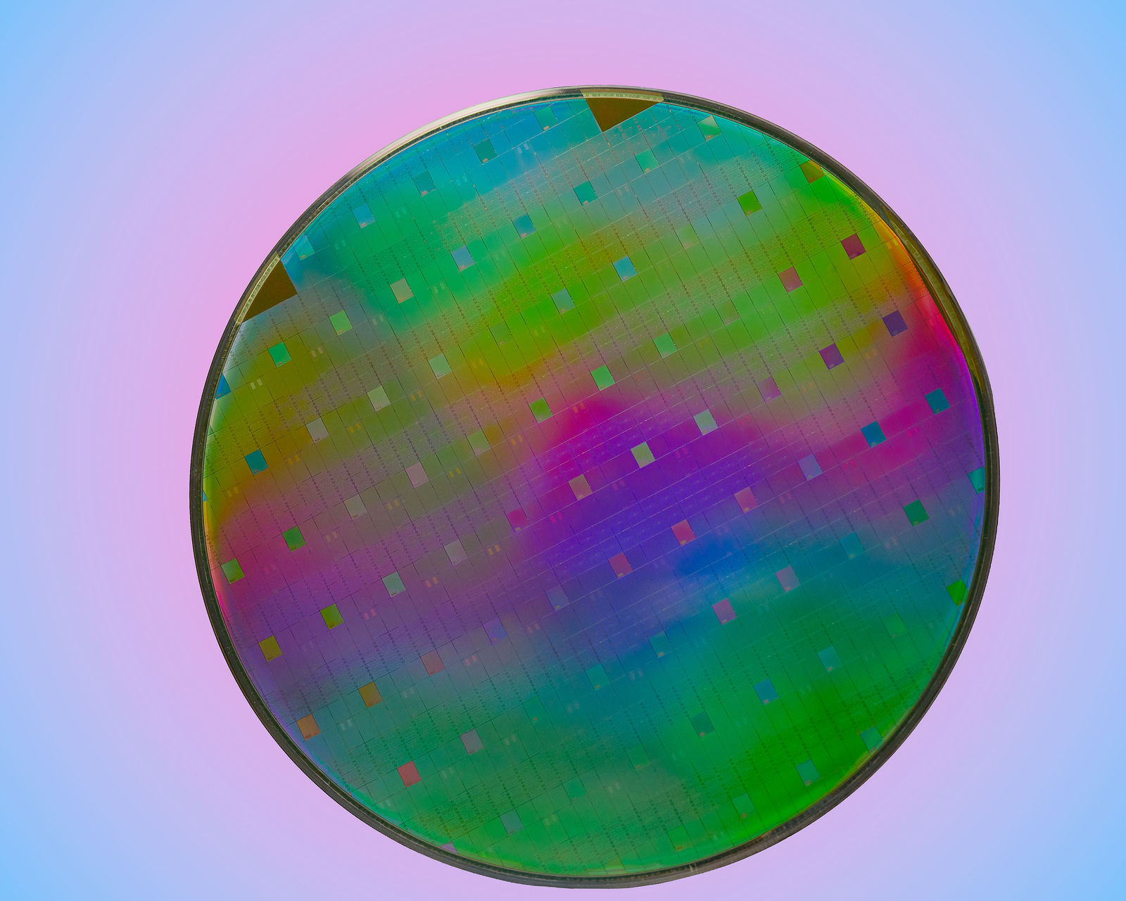
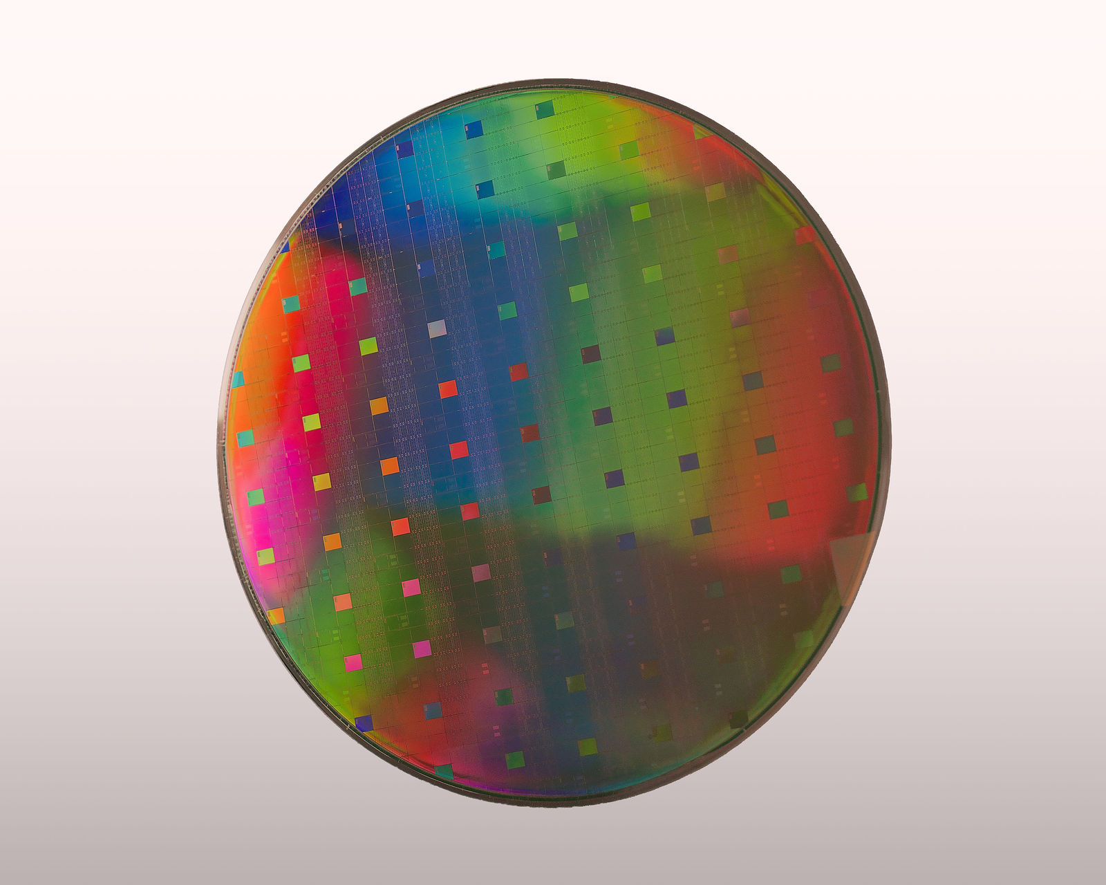
Memory is the biggest binding constraint on AI compute and so we start with a new frontier of AI memory- approaching the bandwidth per watt of SRAM, going up to 10x beyond the capacity of HBM. We use 3D and materials innovations that allow for leapfrogging leading nodes while requiring no EUV lithography and allowing us use fabs that already exist.
Our team co-led one of the industry’s first 3D chip-stacking technologies, has led and scaled seven generations of DRAM and multiple logic designs into billions of chips. We built the world’s first commercial physical synthesis tool and techniques at the heart of the logic design industry and solved long standing challenges in ferroelectrics, invented beyond CMOS logic devices. We would love to work with you to reinvent chip manufacturing here in America.
We have raised $468m, built our own fab and our AI memories sample this year and ramp to production next year. We are allocated for 2027 and will be scaling in America by 2028.
We are open for business, please get in touch to work together. We are also growing the group of Keplerians and would love to work with you.
Learn More @ Kepler: https://keplercompute.com Read our story in @WIRED: https://wired.com/story/a-new-dollar400-million-startup-wants-to-fix-the-ai-memory-bottleneck/…
Kepler — AI’s New Memory
Source: https://keplercompute.com/
AI’s new memory.
Leadership memory beyond HBM & SRAM.
Sampling in 2026. Production in 2027.
A new frontier of bandwidth, capacity and energy
WHO WE ARE
Our team lives and breathes computing across the stack and has created many industry firsts.We have led the development and scaling of technologies to billions of chips across mainstream transistors, 3D logic stacking, seven generations of DRAM, first to market 232-layer NAND, and mobile SoCs. We built the world’s first commercial physical synthesis tool, developed foundational EDA techniques across the industry and have solved long-standing challenges in ferroelectrics and beyond-CMOS devices and memories.
WHAT WE BELIEVE
A different way is possible.
01
Leadership chips without EUV
It is possible to build leadership chips without a dependence on EUV
02
Orders of magnitude more compute per watt
It is possible to achieve multiple orders of magnitude more intelligence per watt by evolving chips 2D Silicon to 3D Beyond silicon
03
Mainstream Digital Computing.
It is possible to get much closer to the physical limits of computing than we are today while staying within mainstream digital computing
WHAT WE OFFER
AI memory for high-throughput, high interactivity inference.
Kepler memory is designed to approach bandwidth per watt of SRAM and go beyond the capacities of SRAM and HBM. Enabling a new frontier of throughput and interactivity for next generation inference
- Bandwidth per watt approaching SRAM.
- Capacity beyond SRAM & HBM.
- Driven by innovations in 3D & Materials
SILICON TO VOLUME
Sampling by year end. Ramping in 2027.
We are working through 2028-30 allocations.
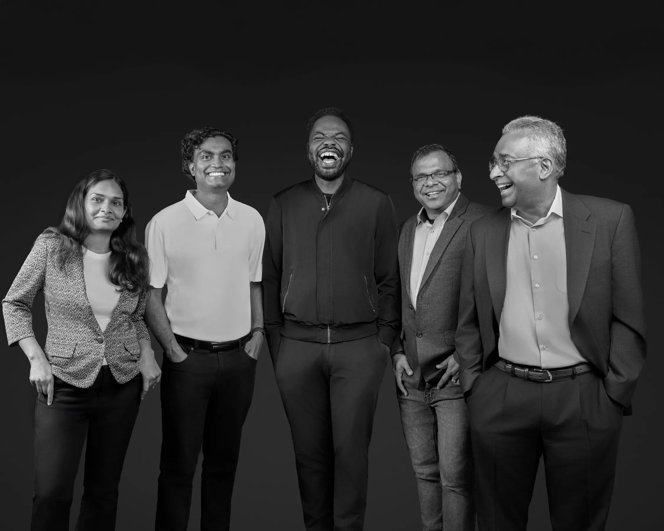 Selected builders across memory, manufacturing, devices and systems
01/02

Sasi Manipatruni
Co-founder & CTO
Founded Intel’s FEINMAN center for next generation logic and co-invented MESO - a candidate spin based Beyond CMOS logic device. Demonstrated First 50 Gb/s silicon micro ring modulator.
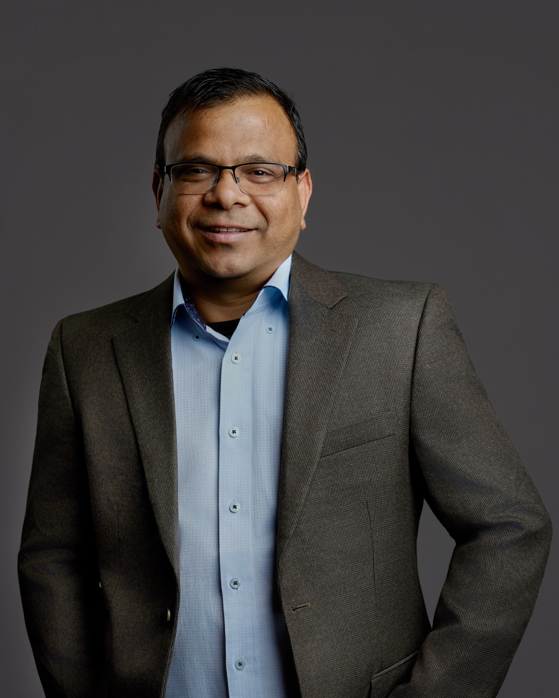
Rajeev Dokania
CO-FOUNDER, CTO, DESIGN & HARDWARE. CHIEF ENGINEERING OFFICER
Co-led definition on Intel Foveros 3D stacking, built high speed circuits that have enabled high volume cpu products
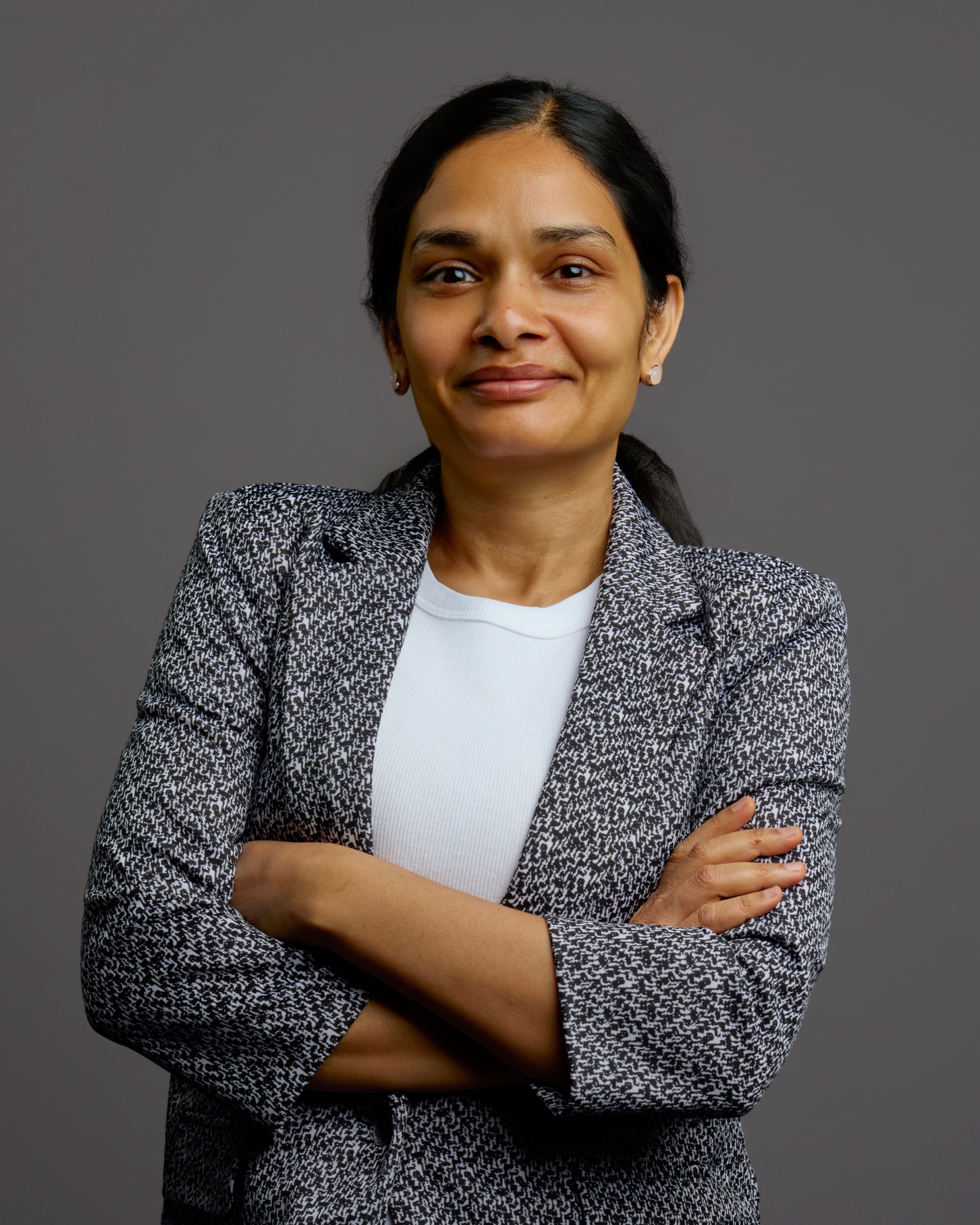
Amrita Mathuriya
Co-founder & CTO, Software & Architecture
Created and scaled CosmoFlow and built computational-lithography software used in Intel’s 14nm process.
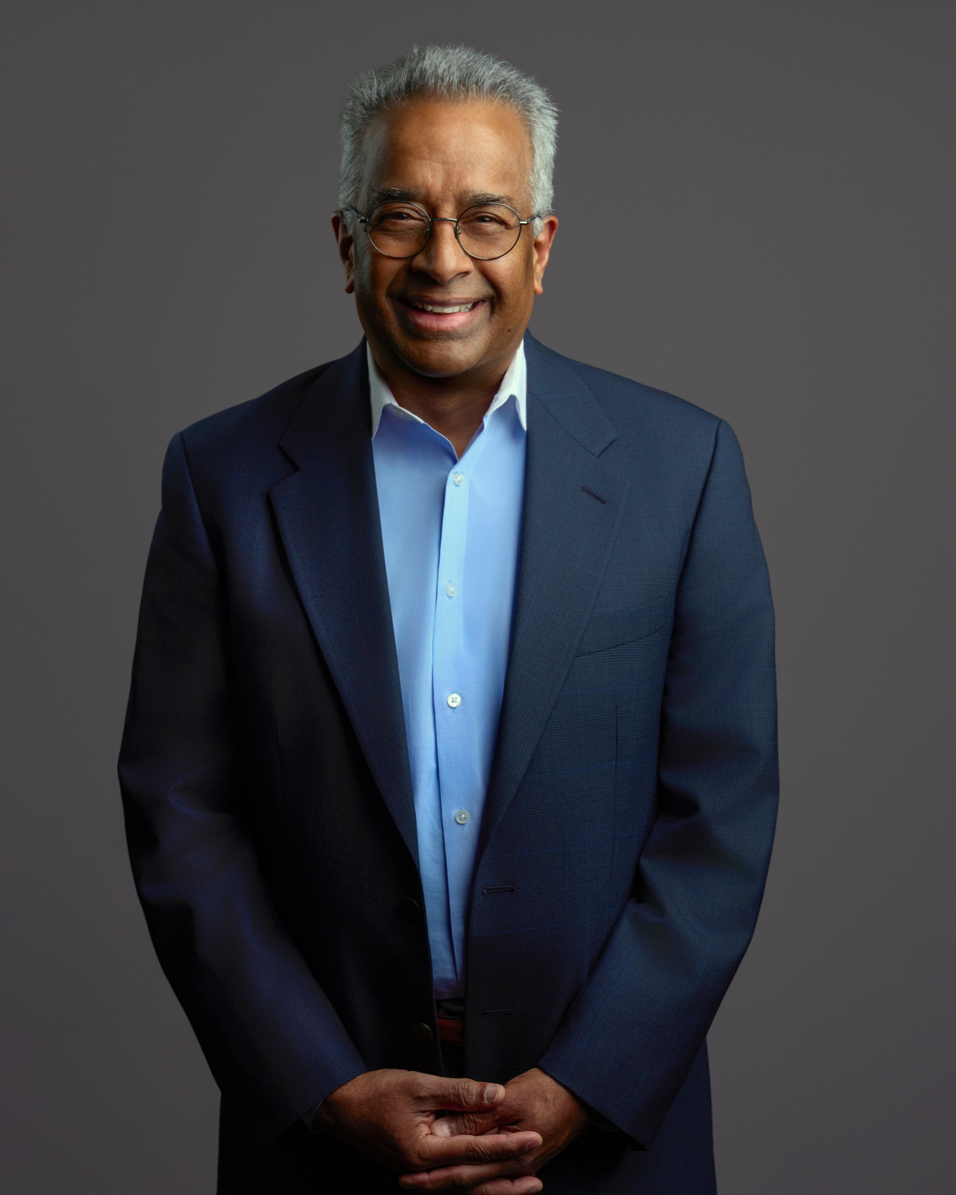
Ramesh Ramamoorthy
Co-founder & Chief Science Officer
Solved long standing problems like fatigue in ferroelectrics, discovered new multiferroic devices for low energy computing

Debo Olaosebikan
Co-founder & CEO
Co-founded Gigster. Demonstrated stimulated emission in work to build a silicon laser during Cornell Physics PhD. Theoretical physics of domain wall motion in spintronics
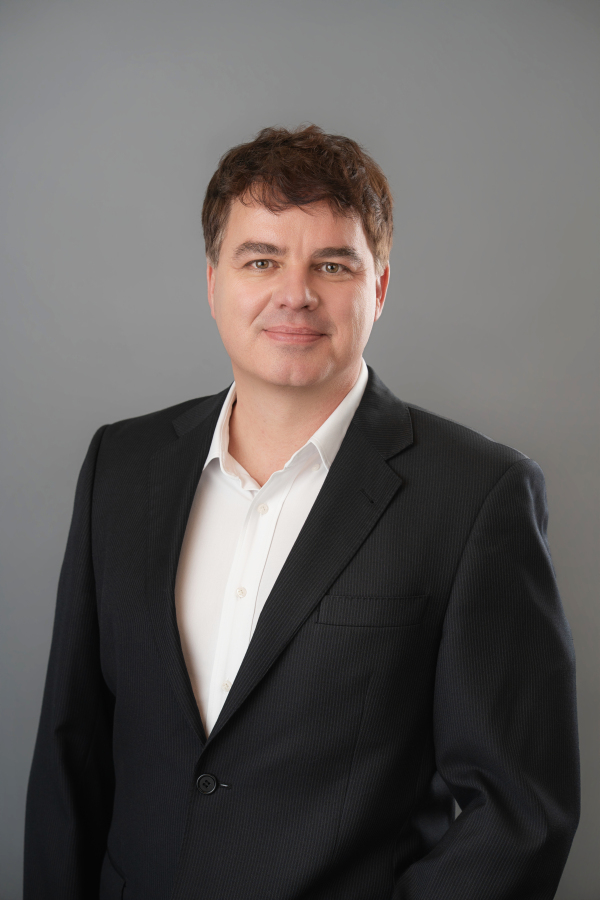
Lars Heineck
MEMORY BU
Scaled seven generations of DRAM to millions of wafers and helped bring first-to-market 232-layer NAND into volume manufacturing.

Noriyuki Sato
PROCESS INTEGRATION
First FInFET integration of SRAM replacement ferroelectrics and led 6 month ramp of a new dedicated 300mm fab from a cold start to electrical data

Sagar Suthram
ADVANCED PACKAGING
Key contributor to world’s first FinFET technology (awarded the Intel Achievement award). Lead inventor for Intel’s precision resistor technology used in high volume manufacturing.

Mauricio Manfrini
MODULES
Led the development and integration of the world’s first 300mm magnetic memory and logic platform.

Antun Domic
PRODUCT & IP
Built world’s first commercial physical synthesis tools that helped establish Synopsys as a leader, from synthesis through automatic layout. Won the 2019 Robert Noyce Medal.
MANUFACTURING LEADERSHIP· sram · DRAM · logic
More intelligence per fab.
Kepler uses the physics of 3D and new materials to produce leadership logic and memory systems that leapfrog EUV only approaches. Allowing for more intelligence per fab and more fabs per dollar
Memory first. Then replace the transistor.
Similar Articles
A Stealth Startup Thinks It Just Hacked the Memory Shortage
Kepler Computing, a stealth startup, has emerged with a new 3D-stacked memory architecture designed to alleviate the global memory shortage for AI applications by increasing density without relying on EUV lithography, backed by substantial funding from investors and the US government.
Progress (3 minute read)
Etched announces breakthroughs in low voltage inference and cluster scale memory for their AI inference hardware, with first racks shipping this summer and $1B in customer contracts.
This chip startup just raised $135M on a bet that AI’s biggest bottleneck isn’t compute — it’s memory
XCENA, a chip startup founded by Samsung and SK Hynix veterans, raised $135M to develop a memory-centric chip that handles AI inference tasks near DRAM, reducing costly data transfers between CPUs and GPUs. The company's MX1 chip is expected to improve efficiency and reduce infrastructure costs.
Neocloud Lambda secures $1B in debt to buy more chips
Lambda raises $1 billion in debt to purchase Nvidia's AI chips for leasing to Microsoft, reflecting the increasing use of debt financing in AI infrastructure.
AI chip startup Etched defies skeptics, hits $10.3B valuation from big-name investors
AI chip startup Etched raised $300M at a $10.3B valuation, defying skeptics by designing specialized chips for AI inference with low-voltage and cluster-scale memory technologies.